LMV324M/NOPB National Semiconductor, LMV324M/NOPB Datasheet - Page 4
LMV324M/NOPB
Manufacturer Part Number
LMV324M/NOPB
Description
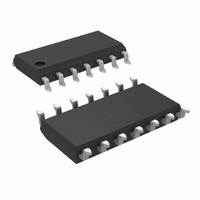
IC OP AMP QUAD LOW V R-R 14-SOIC
Manufacturer
National Semiconductor
Specifications of LMV324M/NOPB
Amplifier Type
General Purpose
Number Of Circuits
4
Output Type
Rail-to-Rail
Slew Rate
1 V/µs
Gain Bandwidth Product
1MHz
Current - Input Bias
15nA
Voltage - Input Offset
1700µV
Current - Supply
410µA
Current - Output / Channel
160mA
Voltage - Supply, Single/dual (±)
2.7 V ~ 5.5 V
Operating Temperature
-40°C ~ 85°C
Mounting Type
Surface Mount
Package / Case
14-SOIC (3.9mm Width), 14-SOL
Bandwidth
1 MHz
Common Mode Rejection Ratio
65
Current, Input Bias
15 nA
Current, Input Offset
5 nA
Current, Output
60 mA
Current, Supply
410 μA
Impedance, Thermal
145 °C/W
Number Of Amplifiers
Quad
Package Type
SOIC-14
Temperature, Operating, Range
-40 to +85 °C
Voltage, Gain
100 V/mV
Voltage, Input
2.7 to 5.5 V
Voltage, Noise
39 nV/sqrt Hz
Voltage, Offset
1.7 mV
Voltage, Supply
5 V
Lead Free Status / RoHS Status
Lead free / RoHS Compliant
-3db Bandwidth
-
Lead Free Status / Rohs Status
RoHS Compliant part
Electrostatic Device
Other names
*LMV324M
*LMV324M/NOPB
LMV324M
*LMV324M/NOPB
LMV324M
Available stocks
Company
Part Number
Manufacturer
Quantity
Price
Company:

Part Number:
LMV324M/NOPB
Manufacturer:
IDT
Quantity:
112


www.national.com
5-Pin SC70
5-Pin SOT23
8-Pin SOIC
8-Pin MSOP
14-Pin SOIC
14-Pin TSSOP
Note 1: Absolute Maximum Ratings indicate limits beyond which damage to the device may occur. Operating Ratings indicate conditions for which the device is
intended to be functional, but specific performance is not guaranteed. For guaranteed specifications and the test conditions, see the Electrical Characteristics.
Note 2: Human Body Model, applicable std. MIL-STD-883, Method 3015.7. Machine Model, applicable std. JESD22-A115-A (ESD MM std. of JEDEC)
Field-Induced Charge-Device Model, applicable std. JESD22-C101-C (ESD FICDM std. of JEDEC
Note 3: Shorting output to V
Note 4: Shorting output to V
Note 5: The maximum power dissipation is a function of T
is P
Note 6: Typical values represent the most likely parametric norm as determined at the time of characterization. Actual typical values may vary over time and will
also depend on the application and configuration. The typical values are not tested and are not guaranteed on shipped production material.
Note 7: All limits are guaranteed by testing or statistical analysis.
Note 8: R
Note 9: Connected as voltage follower with 3V step input. Number specified is the slower of the positive and negative slew rates.
Note 10: All numbers are typical, and apply for packages soldered directly onto a PC board in still air.
Connection Diagrams
Ordering Information
D
= (T
Package
J(MAX)
L
is connected to V
5-Pin SC70/SOT23
– T
A
)/ θ
Top View
JA
. All numbers apply for packages soldered directly onto a PC Board.
+
-
-
. The output voltage is 0.5V
will adversely affect reliability.
will adversely affect reliability.
Temperature Range
−40°C to +85°C
LMV358MMX
LMV324MTX
LMV321M7X
LMV321M5X
LMV358MM
LMV321M7
LMV321M5
LMV358MX
LMV324MX
LMV324MT
10006001
LMV358M
LMV324M
Industrial
≤
J(MAX)
V
O
, θ
≤
JA
4.5V.
Packaging Marking
8-Pin SOIC/MSOP
. The maximum allowable power dissipation at any ambient temperature
LMV324MT
LMV358M
LMV324M
Top View
LMV358
A12
A13
4
10006002
1k Units Tape and Reel
1k Units Tape and Reel
2.5k Units Tape and Reel
3.5k Units Tape and Reel
2.5k Units Tape and Reel
2.5k Units Tape and Reel
3k Units Tape and Reel
3k Units Tape and Reel
1k Units Tape and Reel
Transport Media
Rails
Rails
Rails
14-Pin SOIC/TSSOP
Top View
NSC Drawing
MUA08A
MAA05A
MF05A
MTC14
M08A
M14A
10006003
Related parts for LMV324M/NOPB
Image
Part Number
Description
Manufacturer
Datasheet
Request
R

Part Number:
Description:
Operational Amplifier (Op-Amp) IC
Manufacturer:
National Semiconductor
Datasheet:

Part Number:
Description:
National Semiconductor [8-Bit D/A Converter]
Manufacturer:
National Semiconductor
Datasheet:
Part Number:
Description:
National Semiconductor [Media Coprocessor]
Manufacturer:
National Semiconductor
Datasheet:
Part Number:
Description:
Digitally Controlled Tone and Volume Circuit with Stereo Audio Power Amplifier, Microphone Preamp Stage and National 3D Sound
Manufacturer:
National Semiconductor
Datasheet:
Part Number:
Description:
Digitally Controlled Tone and Volume Circuit with Stereo Audio Power Amplifier, Microphone Preamp Stage and National 3D Sound
Manufacturer:
National Semiconductor
Datasheet:
Part Number:
Description:
AC97 Rev 2 Codec with Sample Rate Conversion and National 3D Sound
Manufacturer:
National Semiconductor
Part Number:
Description:
Manufacturer:
National Semiconductor
Datasheet:
Part Number:
Description:
Manufacturer:
National Semiconductor
Datasheet:
Part Number:
Description:
General Purpose, Low Voltage, Low Power, Rail-to-Rail Output Operational Amplifiers
Manufacturer:
National Semiconductor
Datasheet:
Part Number:
Description:
8-bit 20 MSPS flash A/D converter.
Manufacturer:
National Semiconductor
Datasheet:
Part Number:
Description:
Low Noise Quad Operational Amplifier
Manufacturer:
National Semiconductor
Datasheet:
Part Number:
Description:
Quad Differential Line Receivers
Manufacturer:
National Semiconductor
Datasheet:
Part Number:
Description:
Quad High Speed Trapezoidal? Bus Transceiver
Manufacturer:
National Semiconductor
Datasheet:
Part Number:
Description:
Dual Line Receiver
Manufacturer:
National Semiconductor
Datasheet: