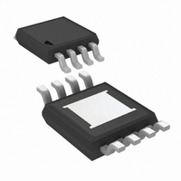
LME49726MY/NOPB National Semiconductor, LME49726MY/NOPB Datasheet - Page 4

LME49726MY/NOPB
Manufacturer Part Number
LME49726MY/NOPB
Description
IC AMP AUDIO STER AB HIFI 8MSOP
Manufacturer
National Semiconductor
Datasheet
1.LME49726MYNOPB.pdf
(22 pages)
Specifications of LME49726MY/NOPB
Amplifier Type
Audio
Number Of Circuits
2
Slew Rate
3.7 V/µs
Gain Bandwidth Product
6.25MHz
Current - Input Bias
0.2pA
Voltage - Input Offset
500µV
Current - Supply
700µA
Current - Output / Channel
350mA
Voltage - Supply, Single/dual (±)
2.5 V ~ 5.5 V, ±1.25 V ~ 2.75 V
Operating Temperature
-40°C ~ 85°C
Mounting Type
Surface Mount
Package / Case
8-MSOP Exposed Pad, 8-HMSOP, 8-eMSOP
Lead Free Status / RoHS Status
Lead free / RoHS Compliant
Output Type
-
-3db Bandwidth
-
Other names
LME49726MYTR
www.national.com
V
I
I
OUT
S
OUTSWING
Note 1: Absolute Maximum Ratings” indicate limits beyond which damage to the device may occur, including inoperability and degradation of device reliability
and/or performance. Functional operation of the device and/or non-degradation at the Absolute Maximum Ratings or other conditions beyond those indicated in
the Recommended Operating Conditions is not implied. The Recommended Operating Conditions indicate conditions at which the device is functional and the
device should not be operated beyond such conditions. All voltages are measured with respect to the ground pin, unless otherwise specified.
Note 2: The Electrical Characteristics tables list guaranteed specifications under the listed Recommended Operating Conditions except as otherwise modified
or specified by the Electrical Characteristics Conditions and/or Notes. Typical specifications are estimations only and are not guaranteed.
Note 3: The maximum power dissipation must be derated at elevated temperatures and is dictated by T
allowable power dissipation is P
Derating curve for additional information.
Note 4: Human body model, applicable std. JESD22-A114C.
Note 5: Machine model, applicable std. JESD22-A115-A.
Note 6: Typical values represent most likely parametric norms at T
characterization and are not guaranteed.
Note 7: Datasheet min/max specification limits are guaranteed by test or statistical analysis.
Symbol
Maximum Output Voltage Swing
Output Current
Quiescent Current per Amplifier
Parameter
DMAX
= (T
JMAX
- T
A
) / θ
JA
or the number given in Absolute Maximum Ratings, whichever is lower. For the LME49726, see Power
R
R
V
V
I
I
OUT
OUT
OUT
OUT
L
L
A
= 2kΩ to V
= 16Ω to V
= 0mA, V
= 0mA, V
= +25ºC, and at the Recommended Operation Conditions at the time of product
= 5V, V
= 2.5V, V
Conditions
4
DD
DD
DD
DD
DD
DD
= 5V
/2
/2
= 5V
= 2.5V
= 2.5V
JMAX
, θ
JA
, and the ambient temperature, T
V
V
V
V
(Note
SS
Typical
DD
DD
SS
0.64
350
160
–0.004
0.7
+0.004
+0.33
–0.33
LME49726
6)
(Note
Limit
1.1
1.0
7)
A
. The maximum
mA (max)
mA (max)
(Limits)
V (max)
V (max)
V (min)
V (min)
Units
mA
mA


