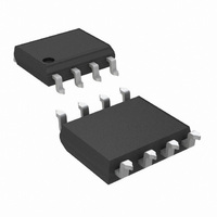
LMV358M/NOPB National Semiconductor, LMV358M/NOPB Datasheet - Page 14

LMV358M/NOPB
Manufacturer Part Number
LMV358M/NOPB
Description
IC OP AMP DUAL LOW V R-R 8-SOIC
Manufacturer
National Semiconductor
Specifications of LMV358M/NOPB
Amplifier Type
General Purpose
Number Of Circuits
2
Output Type
Rail-to-Rail
Slew Rate
1 V/µs
Gain Bandwidth Product
1MHz
Current - Input Bias
15nA
Voltage - Input Offset
1700µV
Current - Supply
210µA
Current - Output / Channel
160mA
Voltage - Supply, Single/dual (±)
2.7 V ~ 5.5 V
Operating Temperature
-40°C ~ 85°C
Mounting Type
Surface Mount
Package / Case
8-SOIC (3.9mm Width)
Bandwidth
1 MHz
Common Mode Rejection Ratio
65
Current, Input Bias
15 nA
Current, Input Offset
5 nA
Current, Output
60 mA
Current, Supply
210 μA
Impedance, Thermal
190 °C/W
Number Of Amplifiers
Dual
Package Type
SOIC-8
Temperature, Operating, Range
-40 to +85 °C
Voltage, Gain
100 V/mV
Voltage, Input
2.7 to 5.5 V
Voltage, Noise
39 nV/sqrt Hz
Voltage, Offset
1.7 mV
Voltage, Supply
5 V
Lead Free Status / RoHS Status
Lead free / RoHS Compliant
-3db Bandwidth
-
Lead Free Status / Rohs Status
RoHS Compliant part
Electrostatic Device
Other names
*LMV358M
*LMV358M/NOPB
LMV358M
*LMV358M/NOPB
LMV358M
Available stocks
Company
Part Number
Manufacturer
Quantity
Price
Company:
Part Number:
LMV358M/NOPB
Manufacturer:
NS
Quantity:
339
Part Number:
LMV358M/NOPB
Manufacturer:
TI/德州仪器
Quantity:
20 000
www.national.com
In
C
margin to the overall system. The desired performance de-
pends on the value of R
the more stable V
of
The circuit in
3
there were a load resistor in
voltage divided by R
ure
techniques to connect V
ing the value of R
LMV358/LMV324. C
of phase margin by feeding the high frequency component of
the output signal back to the amplifier's inverting input, there-
by preserving phase margin in the overall feedback loop.
Increased capacitive drive is possible by increasing the value
of C
FIGURE 5. Indirectly Driving A Capacitive Load with DC
L
because it provides DC accuracy as well as AC stability. If
FIGURE 4. Pulse Response of the LMV324 Circuit in
Figure 3
Figure 3
form a pole to increase stability by adding more phase
5, R
F
. This in turn will slow down the pulse response.
F
provides the DC accuracy by using feed-forward
, the isolation resistor R
using 620Ω for R
Figure 5
F
OUT
due to the input bias current of theLMV321/
ISO
F
will be.
is an improvement to the one in
and R
ISO
and the load resistor. Instead, in
IN
Accuracy
. The bigger the R
Figure 3
to R
ISO
ISO
Figure 4
Figure
L
. Caution is needed in choos-
and 510 pF for C
serve to counteract the loss
ISO
3, the output would be
and the load capacitor
is an output waveform
ISO
10006005
resistor value,
L.
10006099
.
Figure
Fig-
14
INPUT BIAS CURRENT CANCELLATION
The LMV321/LMV358/LMV324 family has a bipolar input
stage. The typical input bias current of LMV321/LMV358/
LMV324 is 15 nA with 5V supply. Thus a 100 kΩ input resistor
will cause 1.5 mV of error voltage. By balancing the resistor
values at both inverting and non-inverting inputs, the error
caused by the amplifier's input bias current will be reduced.
The circuit in
by input bias current.
TYPICAL SINGLE-SUPPLY APPLICATION CIRCUITS
Difference Amplifier
The difference amplifier allows the subtraction of two voltages
or, as a special case, the cancellation of a signal common to
two inputs. It is useful as a computational amplifier, in making
a differential to single-ended conversion or in rejecting a com-
mon mode signal.
FIGURE 6. Cancelling the Error Caused by Input Bias
Figure 6
FIGURE 7. Difference Amplifier
shows how to cancel the error caused
Current
10006006
10006007
10006019


