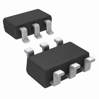
LMH6639MF/NOPB National Semiconductor, LMH6639MF/NOPB Datasheet - Page 15

LMH6639MF/NOPB
Manufacturer Part Number
LMH6639MF/NOPB
Description
IC AMP 190MHZ R-R OTPT SOT23-6
Manufacturer
National Semiconductor
Series
VIP10™r
Datasheet
1.LMH6639MFNOPB.pdf
(20 pages)
Specifications of LMH6639MF/NOPB
Amplifier Type
Voltage Feedback
Number Of Circuits
1
Output Type
Rail-to-Rail
Slew Rate
200 V/µs
Gain Bandwidth Product
90MHz
-3db Bandwidth
228MHz
Current - Input Bias
1.4µA
Voltage - Input Offset
1030µV
Current - Supply
4.18mA
Current - Output / Channel
112mA
Voltage - Supply, Single/dual (±)
3 V ~ 12 V, ±1.5 V ~ 6 V
Operating Temperature
-40°C ~ 85°C
Mounting Type
Surface Mount
Package / Case
SOT-23-6
Number Of Channels
1
Voltage Gain Db
100 dB
Common Mode Rejection Ratio (min)
72 dB
Input Voltage Range (max)
12 V
Input Voltage Range (min)
3 V
Input Offset Voltage
5 mV
Operating Supply Voltage
5 V, 9 V
Supply Current
3.6 mA
Maximum Operating Temperature
+ 85 C
Mounting Style
SMD/SMT
Maximum Dual Supply Voltage
+/- 6 V
Minimum Operating Temperature
- 40 C
Lead Free Status / RoHS Status
Lead free / RoHS Compliant
Other names
LMH6639MF
LMH6639MFTR
LMH6639MFTR
Available stocks
Company
Part Number
Manufacturer
Quantity
Price
Application Notes
INPUT AND OUTPUT TOPOLOGY
All input / output pins are protected against excessive volt-
ages by ESD diodes connected to V+ and V- rails (see
2). These diodes start conducting when the input / output pin
voltage approaches 1V
over voltage. These diodes are normally reverse biased. Fur-
ther protection of the inputs is provided by the two resistors
(R in
diodes connected between both bases of the input stage. The
combination of these resistors and diodes reduces excessive
differential input voltages approaching 2V
mon situation when this occurs is when the device is put in
shutdown and the LMH6639’s inputs no longer follow each
other. In such a case, the diodes may conduct. As a conse-
quence, input current increases, and a portion of signal may
appear at the Hi-Z output. Another possible situation for the
conduction of these diodes is when the LMH6639 is used as
a comparator (or with little or no feedback). In either case, it
is important to make sure that the subsequent current flow
through the device input pins does not violate the Absolute
Maximum Ratings of the device. To limit the current through
the protection circuit extra series resistors can be placed. To-
gether with the build in series resistors of several hundred
ohms this extra resistors can limit the input current to a safe
number depending on the used application. Be aware of the
effect that extra series resistors may impact the switching
speed of the device. A special situation occurs when the part
is configured for a gain of +1, which means the output is di-
rectly connected to the inverting input, see
the part is now placed in shutdown mode the output comes in
a high impedance state and is unable to keep the inverting
input at the same level as the non-inverting input. In many
applications the output is connected to the ground via a low
impedance resistor. When this situation occurs and there is a
DC voltage offset of more than 2 volt between the non-invert-
ing input and the output, current flows from the non-inverting
input through the series resistors R via the bypass diodes to
the output. Now the input current becomes much bigger than
expected and in many cases the source at the input cannot
deliver this current and will drop down. Be sure in this situation
that no DC current path is available from the non-inverting
input to the output pin, or from the output pin to the load re-
Figure
2), in conjunction with the string of anti-parallel
be
beyond V+ or V- to protect against
be
. The most com-
Figure
3. When
Figure
15
sistor. This DC path is drawn by a curved line and can be
broken by placing one of the capacitors C
depending on the used application.
MULTIPLEXING 5 AND 10MHz
The LMH6639 may be used to implement a circuit which mul-
tiplexes two signals of different frequencies. Three LMH6639
high speed op-amps are used in the circuit of
complish the multiplexing function. Two LMH6639 are used
to provide gain for the input signals, and the third device is
used to provide output gain for the selected signal.
FIGURE 3. DC path while in shutdown
FIGURE 2. Input Topology
IN
or C
Figure 4
www.national.com
OUT
20030275
or both,
20030274
to ac-


