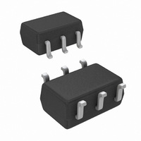
LMV341MG/NOPB National Semiconductor, LMV341MG/NOPB Datasheet - Page 13

LMV341MG/NOPB
Manufacturer Part Number
LMV341MG/NOPB
Description
IC OPAMP 2.7V RRIO SNGL SC70-6
Manufacturer
National Semiconductor
Datasheet
1.LMV341MGNOPB.pdf
(18 pages)
Specifications of LMV341MG/NOPB
Amplifier Type
General Purpose
Number Of Circuits
1
Output Type
Rail-to-Rail
Slew Rate
1 V/µs
Gain Bandwidth Product
1MHz
Current - Input Bias
0.02pA
Voltage - Input Offset
25µV
Current - Supply
107µA
Current - Output / Channel
113mA
Voltage - Supply, Single/dual (±)
2.7 V ~ 5.5 V
Operating Temperature
-40°C ~ 125°C
Mounting Type
Surface Mount
Package / Case
SC-70-6, SC-88, SOT-363
Lead Free Status / RoHS Status
Lead free / RoHS Compliant
-3db Bandwidth
-
Other names
LMV341MG
LMV341MGTR
LMV341MGTR
Available stocks
Company
Part Number
Manufacturer
Quantity
Price
Company:
Part Number:
LMV341MG/NOPB
Manufacturer:
AMD
Quantity:
89
Part Number:
LMV341MG/NOPB
Manufacturer:
NS/国半
Quantity:
20 000
Application Section
LMV341/LMV342/LMV344
The LMV341/LMV342/LMV344 family of amplifiers features
low voltage, low power, and rail-to-rail output operational am-
plifiers designed for low voltage portable applications. The
family is designed using all CMOS technology. This results in
an ultra low input bias current. The LMV341 has a shutdown
option, which can be used in portable devices to increase
battery life.
A simplified schematic of the LMV341/LMV342/LMV344 fam-
ily of amplifiers is shown in Figure 1. The PMOS input differ-
ential pair allows the input to include ground. The output of
this differential pair is connected to the Class AB turnaround
stage. This Class AB turnaround has a lower quiescent cur-
rent, compared to regular turnaround stages. This results in
lower offset, noise, and power dissipation, while slew rate
equals that of a conventional turnaround stage. The output of
the Class AB turnaround stage provides gate voltage to the
complementary common-source transistors at the output
stage. These transistors enable the device to have rail-to-rail
output.
CLASS AB TURNAROUND STAGE AMPLIFIER
This patented folded cascode stage has a combined class AB
amplifier stage, which replaces the conventional folded cas-
code stage. Therefore, the class AB folded cascode stage
runs at a much lower quiescent current compared to conven-
tional folded cascode stages. This results in significantly
smaller offset and noise contributions. The reduced offset and
noise contributions in turn reduce the offset voltage level and
the voltage noise level at the input of the LMV341/LMV342/
LMV344. Also the lower quiescent current results in a high
open-loop gain for the amplifier. The lower quiescent current
does not affect the slew rate of the amplifier nor its ability to
handle the total current swing coming from the input stage.
The input voltage noise of the device at low frequencies, be-
low 1kHz, is slightly higher than devices with a BJT input
stage; However the PMOS input stage results in a much lower
input bias current and the input voltage noise drops at fre-
quencies above 1kHz.
FIGURE 1. Simplified Schematic
20030453
13
SAMPLE AND HOLD CIRCUIT
The lower input bias current of the LMV341 results in a very
high input impedance. The output impedance when the de-
vice is in shutdown mode is quite high. These high
impedances, along with the ability of the shutdown pin to be
derived from a separate power source, make LMV341 a good
choice for sample and hold circuits. The sample clock should
be connected to the shutdown pin of the amplifier to rapidly
turn the device on or off.
Figure 2 shows the schematic of a simple sample and hold
circuit. When the sample clock is high the first amplifier is in
normal operation mode and the second amplifier acts as a
buffer. The capacitor, which appears as a load on the first
amplifier, will be charging at this time. The voltage across the
capacitor is that of the non-inverting input of the first amplifier
since it is connected as a voltage-follower. When the sample
clock is low the first amplifier is shut off, bringing the output
impedance to a high value. The high impedance of this output,
along with the very high impedance on the input of the second
amplifier, prevents the capacitor from discharging. There is
very little voltage droop while the first amplifier is in shutdown
mode. The second amplifier, which is still in normal operation
mode and is connected as a voltage follower, also provides
the voltage sampled on the capacitor at its output.
SHUTDOWN FEATURE
The LMV341 is capable of being turned off in order to con-
serve power and increase battery life in portable devices.
Once in shutdown mode the supply current is drastically re-
duced, 1µA maximum, and the output will be "tri-stated."
The device will be disabled when the shutdown pin voltage is
pulled low. The shutdown pin should never be left unconnect-
ed. Leaving the pin floating will result in an undefined opera-
tion mode and the device may oscillate between shutdown
and active modes.
The LMV341 typically turns on 2.8µs after the shutdown volt-
age is pulled high. The device turns off in less than 400ns after
shutdown voltage is pulled low. Figure 3 and Figure 4 show
the turn-on and turn-off time of the LMV341, respectively. In
order to reduce the effect of the capacitance added to the
circuit by the scope probe, in the turn-off time circuit a resistive
load of 600Ω is added. Figure 5 and Figure 6 show the test
circuits used to obtain the two plots.
FIGURE 2. Sample and Hold Circuit
www.national.com
20030444


