PA02 Cirrus Logic Inc, PA02 Datasheet - Page 2
PA02
Manufacturer Part Number
PA02
Description
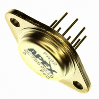
IC PWR AMP 38V 5A 8PIN TO3
Manufacturer
Cirrus Logic Inc
Series
Apex Precision Power™r
Datasheet
1.PA02.pdf
(5 pages)
Specifications of PA02
Amplifier Type
Power
Number Of Circuits
1
Slew Rate
20 V/µs
Gain Bandwidth Product
4.5MHz
Current - Input Bias
50pA
Voltage - Input Offset
5000µV
Current - Supply
27mA
Current - Output / Channel
5A
Voltage - Supply, Single/dual (±)
14 V ~ 38 V, ±7 V ~ 19 V
Operating Temperature
-25°C ~ 85°C
Mounting Type
Through Hole
Package / Case
TO-3-8
Number Of Channels
1
Voltage Gain Db
103 dB
Common Mode Rejection Ratio (min)
70 dB
Input Offset Voltage
10 mV
Maximum Operating Temperature
+ 85 C
Mounting Style
Through Hole
Maximum Dual Supply Voltage
+/- 19 V
Minimum Operating Temperature
- 25 C
Lead Free Status / RoHS Status
Request inventory verification / RoHS Compliant
Output Type
-
-3db Bandwidth
-
Lead Free Status / Rohs Status
Details
Other names
598-1286
Available stocks
Company
Part Number
Manufacturer
Quantity
Price

Part Number:
PA02
Manufacturer:
APEX
Quantity:
20 000
Part Number:
PA0264NL
Manufacturer:
PULSE
Quantity:
20 000
Part Number:
PA0271T
Manufacturer:
PULSE
Quantity:
20 000
Part Number:
PA0277NLT
Manufacturer:
PULSE
Quantity:
20 000
Part Number:
PA0297NL
Manufacturer:
PULSE
Quantity:
20 000


PA02 • PA02A
absolute maXimum ratings
speciFications
PARAMETER
INPUT
OFFSET VOLTAGE, initial
OFFSET VOLTAGE, vs. temperature
OFFSET VOLTAGE, vs. supply
OFFSET VOLTAGE, vs. power
BIAS CURRENT, initial
BIAS CURRENT, vs. temperature
BIAS CURRENT, vs. supply
OFFSET CURRENT, initial
OFFSET CURRENT, vs. temperature
INPUT IMPEDANCE, DC
INPUT CAPACITANCE
COMMON MODE VOLT. RANGE
COMMON MODE VOLT. RANGE
COMMON MODE REJECTION, DC
GAIN
OPEN LOOP GAIN at 10Hz
OPEN LOOP GAIN at 10Hz
GAIN BANDWIDTH PRODUCT at 1MHz T
POWER BANDWIDTH
PHASE MARGIN
OUTPUT
VOLTAGE SWING
VOLTAGE SWING
CURRENT, peak
SETTLING TIME to .1%
SLEW RATE
CAPACITIVE LOAD
HARMONIC DISTORTION
SMALL SIGNAL rise/fall time
SMALL SIGNAL overshoot
POWER SUPPLY
VOLTAGE
CURRENT, quiescent
THERMAL
RESISTANCE, AC junction to case
RESISTANCE, DC junction to case
RESISTANCE, junction to air
TEMPERATURE RANGE, case
NOTES: *
2
caution
1. Long term operation at the maximum junction temperature will result in reduced product life. Derate internal power dissipation to
2. The power supply voltage for all specifications is the TYP rating unless otherwise noted as a test condition.
3. +V
4. Rating applies if the output current alternates between both output transistors at a rate faster than 60Hz.
5. Exceeding CMV range can cause the output to latch.
6. Full temperature specifications are guaranteed but not 100% tested.
7. The absolute maximum negative input voltage is equal to the negative power supply voltage plus 1V (-Vs + 1V).
The specification of PA02A is identical to the specification for PA02 in applicable column to the left.
achieve high MTTF.
S
3
3
and –V
The internal substrate contains beryllia (BeO). Do not break the seal. If accidentally broken, do not crush, machine, or
subject to temperatures in excess of 850°C to avoid generating toxic fumes.
S
denote the positive and negative supply rail respectively. Total V
5
5
, Pos.
, Neg.
4
TEST CONDITIONS
T
Full temperature range
T
T
T
T
T
T
T
T
T
Full temperature range
Full temperature range
Full temperature range
T
Full temp. range, 10kΩ load
T
Full temp. range, 10Ω load
T
Full temp. range, I
T
T
T
Full temp. range, A
P
R
R
Full temperature range
T
F > 60Hz
F < 60Hz
Meets full range specifications
C
C
C
C
C
C
C
C
C
C
C
C
C
C
C
C
C
O
C
L
L
= 10Ω, A
= 25°C
= 25°C
= 25°C
= 25°C
= 85°C
= 25°C
= 25°C
= 85°C
= 25°C
= 25°C
= 25°C, 1kΩ load
= 25°C, 10Ω load
= 25°C, 10Ω load
= 25°C, I
= 25°C
= 25°C, 2V step
= 25°C
= 25°C
= 10Ω, A
= .5W, F = 1kHz, R
V
V
O
SUPPLY VOLTAGE, +V
OUTPUT CURRENT, within SOA
POWER DISSIPATION, internal
INPUT VOLTAGE, differential
INPUT VOLTAGE, common mode
TEMPERATURE, pin solder - 10s
TEMPERATURE, junction
TEMPERATURE RANGE, storage
OPERATING TEMPERATURE RANGE, case
= 1
= 1
= 5A, R
O
V
= 2A
> 10
2, 6
CL
L
= .08Ω
= 10Ω
P r o d u c t I n n o v a t i o n F r o m
S
to –V
1
+V
–V
±V
±V
MIN
–25
70
86
13
±7
S
S
S
S
5
S
–6
+6
–4
–2 ±V
1
+V
–V
±V
S
PA02
1000
SOA
TYP
.004
±10
±10
100
103
100
350
100
±15
.01
4.5
2.4
is measured from +V
S
1.9
±5
±6
50
25
30
20
10
27
30
.6
S
3
S
S
–1.2
–3
+5
–3
MAX
±10
±50
200
200
100
100
±19
+85
2.1
2.6
40
MIN
–55
*
*
*
*
*
*
*
*
*
38V
5A
48W
±30V
–V
300°C
150°C
–65 to +150°C
–55 to +125°C
S
to –V
S
+2V to +V
PA02A
TYP
±1
25
15
*
*
*
*
*
*
*
*
*
*
*
*
*
*
*
*
*
*
*
*
*
*
*
*
*
*
*
S
.
S
MAX
+125
–2V
±25
100
±3
50
*
*
*
*
*
*
UNITS
µV/°C
pA/°C
pA/°C
PA02U
µV/W
°C/W
°C/W
°C/W
µV/V
pA/V
MHz
V/µs
kHz
mV
GΩ
mA
pA
pA
pF
dB
dB
dB
µs
ns
°C
%
%
V
V
V
V
A
V
°
Related parts for PA02
Image
Part Number
Description
Manufacturer
Datasheet
Request
R

Part Number:
Description:
Development Kit
Manufacturer:
Cirrus Logic Inc
Datasheet:
Part Number:
Description:
Development Kit
Manufacturer:
Cirrus Logic Inc
Datasheet:


Part Number:
Description:
High-efficiency PFC + Fluorescent Lamp Driver Reference Design
Manufacturer:
Cirrus Logic Inc
Datasheet:
Part Number:
Description:
Development Kit
Manufacturer:
Cirrus Logic Inc
Datasheet:
Part Number:
Description:
Development Kit
Manufacturer:
Cirrus Logic Inc
Datasheet:

Part Number:
Description:
Development Kit
Manufacturer:
Cirrus Logic Inc
Datasheet:
Part Number:
Description:
Development Kit
Manufacturer:
Cirrus Logic Inc
Datasheet:
Part Number:
Description:
Development Kit
Manufacturer:
Cirrus Logic Inc
Datasheet:
Part Number:
Description:
Development Kit
Manufacturer:
Cirrus Logic Inc
Datasheet:

Part Number:
Description:
EVALUATION BOARD FOR CS8427
Manufacturer:
Cirrus Logic Inc
Datasheet:

Part Number:
Description:
BOARD EVAL FOR CS8416 RCVR
Manufacturer:
Cirrus Logic Inc
Datasheet:

Part Number:
Description:
EVALUATION BOARD FOR CS8420
Manufacturer:
Cirrus Logic Inc
Datasheet:

Part Number:
Description:
KIT DEVELOPMENT EP9315 ARM9
Manufacturer:
Cirrus Logic Inc
Datasheet:

Part Number:
Description:
KIT DEVELOPMENT EP9302 ARM9
Manufacturer:
Cirrus Logic Inc
Datasheet: