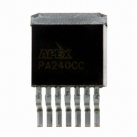
PA240CC Cirrus Logic Inc, PA240CC Datasheet - Page 4

PA240CC
Manufacturer Part Number
PA240CC
Description
IC PWR AMP 350V 120MA 7DDPAK
Manufacturer
Cirrus Logic Inc
Series
Apex Precision Power™r
Specifications of PA240CC
Amplifier Type
Power
Number Of Circuits
1
Slew Rate
30 V/µs
Gain Bandwidth Product
3MHz
Current - Input Bias
50pA
Voltage - Input Offset
25000µV
Current - Supply
2.2mA
Current - Output / Channel
120mA
Voltage - Supply, Single/dual (±)
100 V ~ 350 V, ±50 V ~ 175 V
Operating Temperature
-25°C ~ 85°C
Mounting Type
Surface Mount
Package / Case
TO-263-7, D²Pak (7 leads + Tab), TO-263CA
Number Of Channels
1
Voltage Gain Db
96 dB
Common Mode Rejection Ratio (min)
84 dB
Input Offset Voltage
40 mV
Maximum Operating Temperature
+ 85 C
Mounting Style
SMD/SMT
Maximum Dual Supply Voltage
+/- 175 V
Minimum Operating Temperature
- 25 C
Lead Free Status / RoHS Status
Lead free / RoHS Compliant
Output Type
-
-3db Bandwidth
-
Lead Free Status / Rohs Status
Details
Other names
598-1354
Available stocks
Company
Part Number
Manufacturer
Quantity
Price
Company:
Part Number:
PA240CC
Manufacturer:
RECOM
Quantity:
12 000
Part Number:
PA240CC
Manufacturer:
APEX
Quantity:
20 000
PA240
GENERAL
erations" which covers stability, power supplies, heat sinking,
mounting, current limit, SOA interpretation, and specification
interpretation. Visit www.Cirrus.com for design tools that help
automate tasks such as calculations for stability, internal power
dissipation, current limit, heat sink selection, Apex Precision
Power's complete Application Notes library, Technical Seminar
Workbook and Evaluation Kits.
PHASE COMPENSATION
ing temperature. The PHASE COMPENSATION typical graph
shows closed loop gain and phase compensation capacitor
value relationships for four case temperatures. The curves are
based on achieving a phase margin of 50°. Calculate the high-
est case temperature for the application (maximum ambient
temperature and highest internal power dissipation) before
choosing the compensation. Keep in mind that when working
with small values of compensation, parasitics may play a large
role in performance of the finished circuit. The compensation
capacitor must be rated for at least the total voltage applied
to the amplifier and should be a temperature stable type such
as NPO or COG.
OTHER STABILITY CONCERNS
when choosing compensation. They stem from the fact that
while "gain" is the most commonly used term, β (the feedback
factor) is really what counts when designing for stability.
1. Gain must be calculated as a non-inverting circuit (equal
2. Including a feedback capacitor changes the feedback factor
(parallel combination of the feedback resistor and all input
resistors) should be limited to 5k ohms or less. The amplifier
input capacitance of about 6pF, plus capacitance of connecting
traces or wires and (if used) a socket will cause undesirable
circuit performance and even oscillation if these resistances
are too high. In circuits requiring high resistances, measure or
estimate the total sum point capacitance, multiply by Rin/Rf, and
parallel Rf with this value. Capacitors included for this purpose
are usually in the single digit pF range. This technique results
in equal feedback factor calculations for AC and DC cases. It
does not produce a roll off, but merely keeps β constant over
a wide frequency range. Paragraph 6 of Application Note 19
details suitable stability tests for the finished circuit.
4
Please read Application Note 1 "General Operating Consid-
Open loop gain and phase shift both increase with increas-
There are two important concepts about closed loop gain
As a general rule the DC summing junction impedance
input and feedback resistors can provide a signal gain of
-1, but for calculating offset errors, noise, and stability, this
is a gain of 2).
or gain of the circuit. Consider Rin=4.7k, Rf=47k for a gain
of 11. Compensation of 4.7 to 6.8pF would be reasonable.
Adding 33pF parallel to the 47k rolls off the circuit at 103kHz,
and at 2MHz has reduced gain from 11 to roughly 1.5 and
the circuit is likely to oscillate.
P r o d u c t I n n o v a t i o n F r o m
SAFE OPERATING AREA
second breakdown considerations as in bipolar output stages.
However there are still three distinct limitations:
1. Voltage withstand capability of the transistors.
2. Current handling capability of the die metallization.
3. Temperature of the output MOSFETS.
ing Area graphs). Note that each pulse capability line shows
a constant power level (unlike second breakdown limitations
where power varies with voltage stress). These lines are shown
for a case temperature of 25°C. Pulse stress levels for other
case temperatures can be calculated in the same manner as
DC power levels at different temperatures. The output stage is
protected against transient flyback by the parasitic diodes of
the output stage MOSFET structure. However, for protection
against sustained high energy flyback external fast-recovery
diodes must be used.
HEATSINKING
has a large exposed integrated copper heatslug to which the
monolithic amplifier is directly attached. The PA240CC requires
surface mount techniques of heatsinking. A solder connection
to a copper foil area as defined in Note 5 of Page 2 is recom-
mended for circuit board layouts. This may be adequate heat-
sinking but the large number of variables suggests temperature
measurements to be made on the top of the package. Do not
allow the temperature to exceed 85°C.
The MOSFET output stage of the PA240 is not limited by
These limitations can be seen in the SOA (see Safe Operat-
The PA240CC 7-pin DDPAK surface mountable package
0.005
0.003
0.002
0.001
0.05
0.03
0.02
0.01
1.0
0.5
0.3
0.2
0.1
SUPPLY TO OUTPUT DIFFERENTIAL, V S - V O , (V)
10
20 30
DC, T
DC, T
50
C
C
= 25°C
= 85°C
SOA
100
200 300 500
200mS
300mS
1K
PA240U


