AD549LHZ Analog Devices Inc, AD549LHZ Datasheet - Page 12
AD549LHZ
Manufacturer Part Number
AD549LHZ
Description
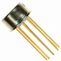
IC OPAMP GP 1MHZ LP 20MA TO99-8
Manufacturer
Analog Devices Inc
Series
Topgate™r
Datasheet
1.AD549JHZ.pdf
(20 pages)
Specifications of AD549LHZ
Slew Rate
3 V/µs
Amplifier Type
General Purpose
Number Of Circuits
1
Gain Bandwidth Product
1MHz
Current - Input Bias
0.04pA
Voltage - Input Offset
300µV
Current - Supply
600µA
Current - Output / Channel
20mA
Voltage - Supply, Single/dual (±)
±5 V ~ 18 V
Operating Temperature
0°C ~ 70°C
Mounting Type
Through Hole
Package / Case
TO-99-8, Metal Can
Op Amp Type
Low Bias Current
No. Of Amplifiers
1
Bandwidth
1MHz
Supply Voltage Range
± 5V To ± 18V
Amplifier Case Style
TO-99
No. Of Pins
8
Lead Free Status / RoHS Status
Lead free / RoHS Compliant
Output Type
-
-3db Bandwidth
-
Lead Free Status / Rohs Status
RoHS Compliant part
Electrostatic Device
Available stocks
Company
Part Number
Manufacturer
Quantity
Price

Part Number:
AD549LHZ
Manufacturer:
ADI/亚德诺
Quantity:
20 000


AD549
AC RESPONSE WITH HIGH VALUE SOURCE AND
FEEDBACK RESISTANCE
Source and feedback resistances greater than 100 kΩ magnify
the effect of the input capacitances (stray and inherent to
the AD549) on the ac behavior of the circuit. The effects of
common-mode and differential input capacitances should be
taken into account because the circuit bandwidth and stability
can be adversely affected.
In a follower, the source resistance and input common-mode
capacitance form a pole that limits the bandwidth to ½πR
Bootstrapping the metal case by connecting Pin 8 to the output
minimizes capacitance due to the package. Figure 32 and Figure 33
show the follower pulse response from a 1 MΩ source resistance
with and without the package connected to the output. Typical
common-mode input capacitance for the AD549 is 0.8 pF.
Figure 32. Follower Pulse Response from 1 MΩ Source Resistance,
Figure 33. Follower Pulse Response from 1 MΩ Source Resistance,
10mV
10mV
Case Not Bootstrapped
Case Bootstrapped
5µs
5µs
S
C
S
Rev. H | Page 12 of 20
.
In an inverting configuration, the differential input capacitance
forms a pole in the loop transmission of the circuit. This can
create peaking in the ac response and possible instability. A
feedback capacitance can be used to stabilize the circuit. The
inverter pulse response with R
in Figure 34. Figure 35 shows the response of the same circuit
with a 1 pF feedback capacitance. Typical differential input
capacitance for the AD549 is 1 pF.
COMMON-MODE INPUT VOLTAGE OVERLOAD
The rated common-mode input voltage range of the AD549 is
from 3 V less than the positive supply voltage to 5 V greater than
the negative supply voltage. Exceeding this range degrades the
CMRR of the amplifier. Driving the common-mode voltage above
the positive supply causes the amplifier output to saturate at the
upper limit of the output voltage. Recovery time is typically 2 μs
after the input has been returned to within the normal operating
range. Driving the input common-mode voltage within 1 V of the
negative supply causes phase reversal of the output signal. In this
case, normal operation typically resumes within 0.5 μs of the
input voltage returning within range.
and Feedback Resistance, 1 pF Feedback Capacitance
Figure 34. Inverter Pulse Response with 1 MΩ Source
Figure 35. Inverter Pulse Response with 1 MΩ Source
10mV
10mV
and Feedback Resistance
F
and R
S
equal to 1 MΩ appears
5µs
5µs
Related parts for AD549LHZ
Image
Part Number
Description
Manufacturer
Datasheet
Request
R

Part Number:
Description:
±1.7g Dual-Axis IMEMS Accelerometer Evaluation Board
Manufacturer:
Analog Devices Inc
Datasheet:

Part Number:
Description:
Inertial Sensor Evaluation System
Manufacturer:
Analog Devices Inc
Datasheet:
Part Number:
Description:
Manufacturer:
Analog Devices Inc
Datasheet:
Part Number:
Description:
Manufacturer:
Analog Devices Inc
Datasheet:
Part Number:
Description:
Manufacturer:
Analog Devices Inc
Datasheet:
Part Number:
Description:
Manufacturer:
Analog Devices Inc
Datasheet:
Part Number:
Description:
Manufacturer:
Analog Devices Inc
Datasheet:
Part Number:
Description:
Manufacturer:
Analog Devices Inc
Datasheet:
Part Number:
Description:
Manufacturer:
Analog Devices Inc
Datasheet:
Part Number:
Description:
Manufacturer:
Analog Devices Inc
Datasheet:
Part Number:
Description:
Manufacturer:
Analog Devices Inc
Datasheet:
Part Number:
Description:
Manufacturer:
Analog Devices Inc
Datasheet:
Part Number:
Description:
Manufacturer:
Analog Devices Inc
Datasheet: