AD600JNZ Analog Devices Inc, AD600JNZ Datasheet
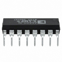
IC AMP VGA DUAL LN 50MA 16DIP

AD600JNZ

Manufacturer Part Number
AD600JNZ
Description
IC AMP VGA DUAL LN 50MA 16DIP
Manufacturer
Analog Devices Inc
Series
X-AMP®r
Datasheets

Specifications of AD600JNZ

Amplifier Type
Variable Gain
Number Of Circuits
2
Slew Rate
275 V/µs
-3db Bandwidth
35MHz
Current - Input Bias
350nA
Current - Supply
11mA
Current - Output / Channel
50mA
Voltage - Supply, Single/dual (±)
±4.75 V ~ 5.25 V
Operating Temperature
0°C ~ 70°C
Mounting Type
Through Hole
Package / Case
16-DIP (0.300", 7.62mm)
No. Of Amplifiers
1
Bandwidth
35MHz
Gain Accuracy
1dB
No. Of Channels
1
Supply Voltage Range
± 4.75V To ± 5.25V
Amplifier Case Style
DIP
No. Of Pins
16
Operating Temperature Range
0°C To
Lead Free Status / RoHS Status
Lead free / RoHS Compliant
Output Type
-
Gain Bandwidth Product
-
Voltage - Input Offset
-
Lead Free Status / RoHS Status
Lead free / RoHS Compliant, Lead free / RoHS Compliant

Available stocks

Company
Part Number
Manufacturer
Quantity
Price
Part Number:
AD600JNZ
Manufacturer:
ADI
Quantity:
422
Part Number:
AD600JNZ
Manufacturer:
ADI/亚德诺
Quantity:
20 000
a
GENERAL DESCRIPTION
The AD600 and AD602 dual channel, low noise, variable gain
amplifiers are optimized for use in ultrasound imaging systems,
but are applicable to any application requiring very precise gain,
low noise and distortion, and wide bandwidth. Each indepen-
dent channel provides a gain of 0 dB to +40 dB in the AD600
and –10 dB to +30 dB in the AD602. The lower gain of the
AD602 results in an improved signal-to-noise ratio at the out-
put. However, both products have the same 1.4 nV/√Hz input
noise spectral density. The decibel gain is directly proportional
to the control voltage, is accurately calibrated, and is supply-
and temperature-stable.
To achieve the difficult performance objectives, a proprietary
circuit form—the X-AMP
nel of the X-AMP comprises a variable attenuator of 0 dB to
–42.14 dB followed by a high speed fixed gain amplifier. In this
way, the amplifier never has to cope with large inputs, and can
benefit from the use of negative feedback to precisely define the
gain and dynamics. The attenuator is realized as a seven-stage
R-2R ladder network having an input resistance of 100 Ω, laser-
trimmed to ±2%. The attenuation between tap points is 6.02 dB;
the gain-control circuit provides continuous interpolation between
these taps. The resulting control function is linear in dB.
*Patented.
REV. D
Information furnished by Analog Devices is believed to be accurate and
reliable. However, no responsibility is assumed by Analog Devices for its
use, nor for any infringements of patents or other rights of third parties that
may result from its use. No license is granted by implication or otherwise
under any patent or patent rights of Analog Devices. Trademarks and
registered trademarks are the property of their respective owners.
FEATURES
2 Channels with Independent Gain Control
2 Gain Ranges:
Accurate Absolute Gain:
Low Input Noise: 1.4 nV/√Hz
Low Distortion: –60 dBc THD at
High Bandwidth: DC to 35 MHz (–3 dB)
Stable Group Delay:
Low Power: 125 mW (Max) per Amplifier
Signal Gating Function for Each Amplifier
Drives High Speed A/D Converters
MIL-STD-883-Compliant and DESC Versions Available
APPLICATIONS
Ultrasound and Sonar Time-Gain Control
High Performance Audio and RF AGC Systems
Signal Measurement
"Linear in dB" Gain Response
AD600: 0 dB to 40 dB
AD602: –10 dB to +30 dB
®
2 ns
—has been developed. Each chan-
0.3 dB
1 V Output
The gain-control interfaces are fully differential, providing an
input resistance of ~15 MΩ and a scale factor of 32 dB/V (that
is, 31.25 mV/dB) defined by an internal voltage reference. The
response time of this interface is less than 1 µs. Each channel
also has an independent gating facility that optionally blocks
signal transmission and sets the dc output level to within a few
millivolts of the output ground. The gating control input is TTL
and CMOS compatible.
The maximum gain of the AD600 is 41.07 dB, and that of the
AD602 is 31.07 dB; the –3 dB bandwidth of both models is
nominally 35 MHz, essentially independent of the gain. The
signal-to-noise ratio (SNR) for a 1 V rms output and a 1 MHz
noise bandwidth is typically 76 dB for the AD600 and 86 dB for
the AD602. The amplitude response is flat within ± 0.5 dB from
100 kHz to 10 MHz; over this frequency range the group delay
varies by less than ± 2 ns at all gain settings.
Each amplifier channel can drive 100 Ω load impedances with
low distortion. For example, the peak specified output is ± 2.5 V
minimum into a 500 Ω load, or ± 1 V into a 100 Ω load. For a
200 Ω load in shunt with 5 pF, the total harmonic distortion for
a ± 1 V sinusoidal output at 10 MHz is typically –60 dBc.
The AD600J and AD602J are specified for operation from 0°C
to 70°C, and are available in both 16-lead plastic DIP (N) and
16-lead SOIC (R) packages. The AD600A and AD602A are
specified for operation from –40°C to +85°C and are available in
both 16-lead Cerdip (Q) and 16-lead SOIC (R) packages.
The AD600S and AD602S are specified for operation from
–55°C to +125°C, are available in a 16-lead Cerdip (Q) package,
and are MIL-STD-883 compliant. The AD600S and AD602S
are also available under DESC SMD 5962-94572.
One Technology Way, P.O. Box 9106, Norwood, MA 02062-9106, U.S.A.
Tel: 781/329-4700
Fax: 781/326-8703
A1LO
C1LO
C1HI
A1HI
0dB
500
GAIN CONTROL
V
G
REFERENCE
INTERFACE
SCALING
–6.02dB
Dual, Low Noise, Wideband
R-2R LADDER NETWORK
FUNCTIONAL BLOCK DIAGRAM
–12.04dB
Variable Gain Amplifiers
–18.06dB
© 2004 Analog Devices, Inc. All rights reserved.
PRECISION PASSIVE
INPUT ATTENUATOR
–22.08dB
–30.1dB
AD600/AD602
–36.12dB
–42.14dB
62.5
INTERFACE
RF1
20
41.07dB(AD600)
2.24k (AD600)
GATING
694 (AD602)
31.07(AD602)
FIXED-GAIN
AMPLIFIER
GAT1
www.analog.com
RF2
*
A1OP
A1CM

Related parts for AD600JNZ

AD600JNZ Summary of contents

Page 1

FEATURES 2 Channels with Independent Gain Control "Linear in dB" Gain Response 2 Gain Ranges: AD600 AD602: – +30 dB Accurate Absolute Gain: 0.3 dB Low Input Noise: 1.4 nV/√Hz Low Distortion: ...

Page 2

AD600/AD602–SPECIFICATIONS +625 mV 500 , and pF, unless otherwise noted. Specifications for the AD600 and AD602 are identical unless otherwise noted Parameter Conditions INPUT CHARACTERISTICS Input Resistance Pins Pins 6 ...

Page 3

ABSOLUTE MAXIMUM RATINGS Supply Voltage ± ± 7 Input ...

Page 4

AD600/AD602–Typical Performance Characteristics 0.45 0.35 0.25 0.15 0.05 –0.05 –0.15 –0.25 –0.35 –0.45 –0.7 –0.5 –0.3 –0.1 0.1 0.3 0.5 0.7 GAIN CONTROL VOLTAGE – V TPC 1. Gain Error vs. Gain Control Voltage 10.0 9.8 9.6 9.4 9.2 9.0 ...

Page 5

TPC 10. Gating Feedthrough to Output, Gating Off to On 500mV 100 200ns TPC 13. Input Stage Overload Recovery Time 10 AD600 20dB 5 AD602 ...

Page 6

AD600/AD602 THEORY OF OPERATION The AD600 and AD602 have the same general design and features. They comprise two fixed gain amplifiers, each pre- ceded by a voltage-controlled attenuator 42.14 dB with independent control interfaces, each having ...

Page 7

The Gain-Control Interface The attenuation is controlled through a differential, high imped- ance (15 MΩ) input, with a scaling factor that is laser trimmed per volt, that is, 31.25 mV/dB. Each of the two amplifiers has its ...

Page 8

AD600/AD602 –40.00dB INPUT 0dB C1HI –0.51dB INPUT 0dB C1HI V = 1.25V C INPUT 0dB C1HI V = 2.5V C Figure 3. AD600 Gain Control Input Calculations for Sequential Control Operation The gains are offset (Figure ...

Page 9

A1 30 COMBINED –10 –0.5 0.0 0.5 1.0 1 Figure 5. Plot of Separate and Overall Gains in Sequential Control –1 –2 –3 ...

Page 10

AD600/AD602 APPLICATIONS The full potential of any high performance amplifier can only be realized by careful attention to details in its applications. The following pages describe fully tested circuits in which many such details have already been considered. However, as ...

Page 11

GAIN-CONTROL VOLTAGE V G – + C1LO C1HI 1 16 A1CM A1HI A1OP A1LO 3 14 – VPOS GAT1 4 13 REF V IN VNEG GAT2 5 12 A2LO A2OP 6 11 – A2 A2CM A2HI ...

Page 12

AD600/AD602 5V R3 46.4k R4 3.74k C1LO 1 A1HI INPUT A1 A1LO 3 – GAT1 4 REF GAT2 5 A2LO 6 – A2 A2HI 7 + C2LO 8 AD600 Figure 15. This Accurate HF AGC Amplifier Uses ...

Page 13

FREQUENCY – MHz Figure 16. AC Response at the Stabilized Output Level of 1.3 V RMS +0.2 0 –0.2 –0.4 0.001 0.01 INPUT AMPLITUDE – V RMS Figure 17. Output Stabilization vs. RMS Input for Sine Wave ...

Page 14

AD600/AD602 CAL 0dB C1LO 1 R1 INPUT 115 A1HI 1V RMS 2 MAX R2 200 (SINE WAVE) A1LO 3 GAT1 4 GAT2 R3 5 133k A2LO 6 A2HI U3A 7 C2LO 1/2 8 AD712 15.625mV/dB 3.01k Figure ...

Page 15

X-AMP. Note that it occurs with a periodicity of 12 dB—twice the separation between the tap points (because of the two cascaded stages –1 –2 –3 –4 –5 ...

Page 16

AD600/AD602 C1LO 1 INPUT A1HI 1V RMS 2 + MAX A1 A1LO (SINE WAVE) 3 – GAT1 4 REF GAT2 5 A2LO 6 – A2 A2HI 7 + C2LO 8 U1 AD600 +5V FB 0.1 F +5V DEC 0.1 F ...

Page 17

INPUT SIGNAL – V RMS Figure 27. Gain Error for Figure 19 without the 2 dB Offset Modification 2.0 1.5 1.0 0.5 0.1 0 ...

Page 18

AD600/AD602 0dB ADJUST C1LO R3 1 R17 200 INPUT 115 A1HI 2 + A1LO 3 – GAT1 4 GAT2 5 A2LO 6 – A2 A2HI 7 + C2LO 8 U1 AD600 +6V FB 0.1 F +6V DEC 0.1 F –6V ...

Page 19

INPUT SIGNAL – V RMS Figure 31. Error Ripple Due to the Individual Gain Functions 400 350 300 250 200 1 10 100 1m ...

Page 20

AD600/AD602 Dimensions shown in inches and (mm) 16-Lead Plastic DIP Package (N-16) 0.785 (19.94) 0.765 (19.43) 0.295 (7.49) 0.745 (18.92) 0.285 (7.24) 0.275 (6.99 0.100 (2.54) BSC 0.015 (0.38) MIN 0.180 (4.57) MAX 0.150 (3.81) 0.130 ...

Page 21

Revision History Location 3/04—Data Sheet changed from REV REV. D. Changes to SPECIFICATIONS . . . . . . . . . . . . . . . . . . . . . . . . . ...

Page 22

–22– ...

Page 23

–23– ...

Page 24

–24– ...

Related keywords