OP77FJZ Analog Devices Inc, OP77FJZ Datasheet - Page 11
OP77FJZ
Manufacturer Part Number
OP77FJZ
Description
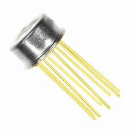
IC OPAMP GP 600KHZ PREC TO99-8
Manufacturer
Analog Devices Inc
Datasheet
1.OP77FZ.pdf
(16 pages)
Specifications of OP77FJZ
Slew Rate
0.3 V/µs
Amplifier Type
General Purpose
Number Of Circuits
1
Gain Bandwidth Product
600kHz
Current - Input Bias
1.2nA
Voltage - Input Offset
20µV
Voltage - Supply, Single/dual (±)
±3 V ~ 18 V
Operating Temperature
-25°C ~ 85°C
Mounting Type
Through Hole
Package / Case
TO-99-8, Metal Can
Op Amp Type
Low Offset Voltage
No. Of Amplifiers
1
Bandwidth
600kHz
Supply Voltage Range
± 3V To ± 18V
Amplifier Case Style
TO-99
No. Of Pins
8
Lead Free Status / RoHS Status
Lead free / RoHS Compliant
Current - Supply
-
Output Type
-
Current - Output / Channel
-
-3db Bandwidth
-
Lead Free Status / RoHS Status
Lead free / RoHS Compliant, Lead free / RoHS Compliant


APPLICATIONS
The high gain, gain linearity, CMRR, and low TCV
OP77 make it possible to obtain performance not previously
available in single-stage, very high-gain amplifier applications.
For best CMR,
10 mV differential signal, the maximum errors are as listed in
Table 7.
Table 7. Maximum Errors
Type
Common-Mode Voltage
Gain Linearity, Worst Case
TCV
TCI
This circuit reduces maximum slew rate but allows driving
capacitive loads of any size without instability. Because the boon
resistor is inside the feedback loop, its effect on output
impedance is reduced to insignificance by the high open-loop
gain of the OP77.
OS
OS
INPUT
Figure 27. Precision High-Gain Differential Amplifier
V
IN
Figure 28. Isolating Large Capacitive Loads
R
100kΩ
100kΩ
R
R
S
R1
R2
1
2
1kΩ
1kΩ
Figure 29. Basic Current Source
R1
R3
must equal
10µF
2
3
2
3
OP77
+15V
–15V
OP77
R4
1MΩ
2
3
4
7
0.1µF
0.1µF
OP77E
990Ω
R
1kΩ
R3
R4
+15V
–15V
F
1MΩ
6
R2
7
4
R
R
0.1µF
0.1µF
6
3
4
. In this example, with a
6
100Ω
R5
10Ω
I
OUT
Amount
0.01%/V
0.02%
0.003%/°C
0.008%/°C
< 15mA
C
LOAD
OUTPUT
OS
of the
Rev. E | Page 11 of 16
These current sources can supply both positive and negative
current into a grounded load.
Note that
And that for Z
V
IN
Z
O
=
R1
R2
R
R
5
5
R
⎛
⎜
⎝
O
+
2
3
2
R
R
to be infinite
R
4
2
OP77
Figure 30. 100 mA Current Source
4
I
GIVEN R3 = R4 + R5, R1 = R2
OUT
+
R
R
1
3
1
⎞
⎟
⎠
= V
IN
6
(
R3
R4
R1 – R5
R3
R +
5
R
)
2
+15V
–15V
R
2N2222
2N2907
4
must =
R5
I
OUT
R
R
3
1
< 100mA
OP77
Related parts for OP77FJZ
Image
Part Number
Description
Manufacturer
Datasheet
Request
R

Part Number:
Description:
IC OPAMP INSTR PREC SGL 8SOIC
Manufacturer:
Linear Technology
Datasheet:

Part Number:
Description:
Op Amps Low-noise op amp Noise Wide-Band Ampl
Manufacturer:
Maxim Integrated Products
Datasheet:

Part Number:
Description:
Op Amps LW-POW SNGL/DUAL R-R I/O OP AMPS
Manufacturer:
Maxim Integrated Products
Datasheet:
Part Number:
Description:
Op Amps LW-POW SNGL/DUAL R-R I/O OP AMPS
Manufacturer:
Maxim Integrated Products
Datasheet:

Part Number:
Description:
Op Amps Dual Op amp JFET
Manufacturer:
Fairchild Semiconductor
Datasheet:

Part Number:
Description:
Op Amps 1.8V 15MHz Low-Offse set Op Amp with RRIO
Manufacturer:
Maxim Integrated Products
Datasheet:

Part Number:
Description:
Op Amps Ultra low-power op a mp in 6-bump WLP pac
Manufacturer:
Maxim Integrated Products
Datasheet:
Part Number:
Description:
Op Amps 1.8V 15MHz Low-Offse set Op Amp with RRIO
Manufacturer:
Maxim Integrated Products
Datasheet:

Part Number:
Description:
Op Amps Dual High-Voltage Op Amp
Manufacturer:
Maxim Integrated Products
Datasheet:


