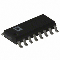
AD8024ARZ Analog Devices Inc, AD8024ARZ Datasheet - Page 10

AD8024ARZ
Manufacturer Part Number
AD8024ARZ
Description
IC OPAMP CF QUAD LP 50MA 16SOIC
Manufacturer
Analog Devices Inc
Datasheet
1.AD8024ARZ.pdf
(12 pages)
Specifications of AD8024ARZ
Slew Rate
390 V/µs
Amplifier Type
Current Feedback
Number Of Circuits
4
-3db Bandwidth
200MHz
Current - Input Bias
1µA
Voltage - Input Offset
2000µV
Current - Supply
16mA
Current - Output / Channel
50mA
Voltage - Supply, Single/dual (±)
5 V ~ 24 V, ±2.5 V ~ 12 V
Operating Temperature
-40°C ~ 85°C
Mounting Type
Surface Mount
Package / Case
16-SOIC (3.9mm Width)
Op Amp Type
High Speed
No. Of Amplifiers
4
Bandwidth
350MHz
Supply Voltage Range
5V To 24V
Amplifier Case Style
SOIC
No. Of Pins
16
Lead Free Status / RoHS Status
Lead free / RoHS Compliant
Output Type
-
Gain Bandwidth Product
-
Lead Free Status / RoHS Status
Lead free / RoHS Compliant, Lead free / RoHS Compliant
Available stocks
Company
Part Number
Manufacturer
Quantity
Price
Part Number:
AD8024ARZ
Manufacturer:
ADI/亚德诺
Quantity:
20 000
AD8024
Overload Recovery
The most important overload conditions are:
When configured for a low closed-loop gain, the AD8024
recovers quickly from an input common-mode voltage over-
drive; typically in <25 ns.
When configured for a higher gain and overloaded at the output,
recovery from an output voltage overdrive is also short; approxi-
mately 55 ns (see Figure 5). For higher overdrive, the response
is somewhat slower. For 100% overdrive, the recovery time is
substantially longer.
When configured for a high noninverting gain, a high input over-
drive can result in a large current into the input stage. Although
this current is internally limited to approximately 30 mA, its
effect on the total power dissipation may be significant. See also
the warning under Maximum Power Dissipation.
Input Common-Mode Voltage Overdrive
Output Voltage Overdrive
Input Current Overdrive.
1V
5V
Ω
V
V
IN
OUT
Ω
±
50ns
Disable Mode Operation
When the Disable pin is tied to DGND, all amplifiers are opera-
tional, in the enabled state.
When the voltage on the Disable pin is raised to 1.6 V or more
above DGND, all amplifiers are in the disabled, powered-down
state. In this condition, the DISABLE pin sources approximately
0.1 µA, the total quiescent current is reduced to approximately
500 µA, all outputs are in a high impedance state, and there is a
high level of isolation from inputs to outputs.
The output impedance in the disabled mode is the equivalent of all
external resistors, seen from the output pin, in parallel with the
total disabled output impedance of the amplifier, typically 20 pF.
The input stages of the AD8024 include protection from large
differential input voltages that may be present in the disabled
mode. Internal clamps limit this voltage to 1.5 V. The high input-
to-output isolation is maintained for voltages below this limit.


