OP400GPZ Analog Devices Inc, OP400GPZ Datasheet - Page 2
OP400GPZ
Manufacturer Part Number
OP400GPZ
Description
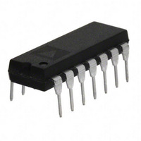
IC OPAMP GP 500KHZ QUAD LP 14DIP
Manufacturer
Analog Devices Inc
Specifications of OP400GPZ
Slew Rate
0.15 V/µs
Amplifier Type
General Purpose
Number Of Circuits
4
Gain Bandwidth Product
500kHz
Current - Input Bias
750pA
Voltage - Input Offset
80µV
Current - Supply
600µA
Voltage - Supply, Single/dual (±)
±3 V ~ 18 V
Operating Temperature
0°C ~ 70°C
Mounting Type
Through Hole
Package / Case
14-DIP (0.300", 7.62mm)
Op Amp Type
General Purpose
No. Of Amplifiers
4
Bandwidth
500kHz
Supply Voltage Range
± 3V To ± 18V
Amplifier Case Style
DIP
No. Of Pins
14
Channel Separation
135
Common Mode Rejection Ratio
135
Current, Input Bias
0.75 nA
Current, Input Offset
0.1 nA
Current, Supply
600 μA
Impedance, Thermal
33 °C/W
Number Of Amplifiers
Quad
Package Type
PDIP-14
Resistance, Input
10 Megohms (Differential), 200 Gigaohms (Common-Mode)
Temperature, Operating, Range
0 to +70 °C
Voltage, Gain
7000 V/mV
Voltage, Input
±13 V
Voltage, Noise
22 nV/sqrt Hz
Voltage, Offset
80 μV
Voltage, Output, High
+12.6 V
Voltage, Output, Low
-12.6 V
Voltage, Supply
±15 V
Lead Free Status / RoHS Status
Lead free / RoHS Compliant
Output Type
-
Current - Output / Channel
-
-3db Bandwidth
-
Lead Free Status / Rohs Status
RoHS Compliant part
Electrostatic Device
Available stocks
Company
Part Number
Manufacturer
Quantity
Price

Part Number:
OP400GPZ
Manufacturer:
ADI/亚德诺
Quantity:
20 000


OP400
TABLE OF CONTENTS
Features .............................................................................................. 1
Functional Block Diagrams ............................................................. 1
General Description ......................................................................... 1
Revision History ............................................................................... 2
Specifications ..................................................................................... 3
Absolute Maximum Ratings ............................................................ 5
REVISION HISTORY
2/11—Rev. F to Rev. G
Added S Package to Storage Temperature Range in Table 4 ....... 5
Updated Outline Dimensions ....................................................... 15
12/08—Rev. E to Rev. F
Added New Figure 28, Renumbered Sequentially ..................... 10
Updated Outline Dimensions ....................................................... 15
1/07—Rev. D to Rev. E
Updated Format .................................................................. Universal
Changes to Figure 1 and Figure 2 ................................................... 1
Removed Figure 4 ............................................................................. 4
Changes to Table 3 ............................................................................ 4
Changes to Figure 16 through Figure 19, Figure 21..................... 8
Changes to Figure 27 ........................................................................ 9
Changes to Figure 28 ...................................................................... 10
Changes to Figure 33 ...................................................................... 13
Updated Outline Dimensions ....................................................... 14
3/06—Rev. C to Rev. D
Updated Format .................................................................. Universal
Deleted Wafer Test Limits Table ..................................................... 4
New Package Drawing: R-14 ......................................................... 15
Updated Outline Dimensions ....................................................... 15
Changes to Ordering Guide .......................................................... 16
Electrical Characteristics ............................................................. 3
Thermal Resistance ...................................................................... 5
ESD Caution .................................................................................. 5
Rev. G | Page 2 of 16
Typical Performance Characteristics ..............................................6
Applications ..................................................................................... 11
Outline Dimensions ....................................................................... 14
6/03—Rev. B to Rev. C
Edits to Specifications ....................................................................... 2
10/02—Rev. A to Rev. B
Addition of Absolute Maximum Ratings ....................................... 5
Edits to Outline Dimensions......................................................... 12
4/02—Rev. 0 to Rev. A
Edits to Features................................................................................. 1
Edits to Ordering Information ........................................................ 1
Edits to Pin Connections .................................................................. 1
Edits to General Descriptions ..................................................... 1, 2
Edits to Package Type ....................................................................... 2
Dual Low Power Instrumentation Amplifier ......................... 11
Bipolar Current Transmitter ..................................................... 12
Differential Output Instrumentation Amplifier .................... 12
Multiple Output Tracking Voltage Reference ......................... 13
Ordering Guide .......................................................................... 15
SMD Parts and Equivalents ...................................................... 15
Related parts for OP400GPZ
Image
Part Number
Description
Manufacturer
Datasheet
Request
R

Part Number:
Description:
±1.7g Dual-Axis IMEMS Accelerometer Evaluation Board
Manufacturer:
Analog Devices Inc
Datasheet:

Part Number:
Description:
Inertial Sensor Evaluation System
Manufacturer:
Analog Devices Inc
Datasheet:
Part Number:
Description:
Manufacturer:
Analog Devices Inc
Datasheet:
Part Number:
Description:
Manufacturer:
Analog Devices Inc
Datasheet:
Part Number:
Description:
Manufacturer:
Analog Devices Inc
Datasheet:
Part Number:
Description:
Manufacturer:
Analog Devices Inc
Datasheet:
Part Number:
Description:
Manufacturer:
Analog Devices Inc
Datasheet:
Part Number:
Description:
Manufacturer:
Analog Devices Inc
Datasheet:
Part Number:
Description:
Manufacturer:
Analog Devices Inc
Datasheet:
Part Number:
Description:
Manufacturer:
Analog Devices Inc
Datasheet:
Part Number:
Description:
Manufacturer:
Analog Devices Inc
Datasheet:
Part Number:
Description:
Manufacturer:
Analog Devices Inc
Datasheet:
Part Number:
Description:
Manufacturer:
Analog Devices Inc
Datasheet: