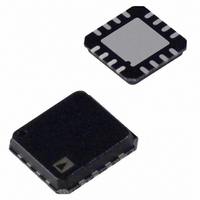
AD8231ACPZ-R7 Analog Devices Inc, AD8231ACPZ-R7 Datasheet

AD8231ACPZ-R7
Specifications of AD8231ACPZ-R7
AD8231ACPZ-R7TR
Q3240237
Available stocks
Related parts for AD8231ACPZ-R7
AD8231ACPZ-R7 Summary of contents
Page 1
FEATURES Digitally/pin-programmable gain 16, 32, 64, or 128 Specified from −40°C to +125°C 50 nV/°C maximum input offset drift 10 ppm/°C maximum gain drift Excellent dc performance 80 dB minimum CMR ...
Page 2
AD8231 TABLE OF CONTENTS Features .............................................................................................. 1 Applications....................................................................................... 1 Functional Block Diagram .............................................................. 1 General Description ......................................................................... 1 Revision History ............................................................................... 2 Specifications..................................................................................... 3 Absolute Maximum Ratings............................................................ 7 Thermal Resistance ...................................................................... 7 Maximum Power Dissipation ..................................................... 7 ESD Caution.................................................................................. 7 ...
Page 3
SPECIFICATIONS 2 kΩ REF L Table 2. Parameter INSTRUMENTATION AMPLIFIER Offset Voltage Input Offset, V OSI Average Temperature Drift Output Offset, V OSO Average Temperature ...
Page 4
AD8231 Parameter Dynamic Performance Bandwidth Gain Bandwidth Product 128 Slew Rate Output Characteristics Output Voltage High Output Voltage Low Short-Circuit Current Digital Interface Input Voltage Low Input Voltage High Setup ...
Page 5
25° REF A Table 3. Parameter INSTRUMENTATION AMPLIFIER Offset Voltage Input Offset, V OSI Average Temperature Drift Output Offset, V OSO Average Temperature Drift Input ...
Page 6
AD8231 Parameter Dynamic Performance Bandwidth Gain Bandwidth Product 128 Slew Rate Output Characteristics Output Voltage High Output Voltage Low Short-Circuit Current Digital Interface Input Voltage Low Input Voltage High Setup ...
Page 7
ABSOLUTE MAXIMUM RATINGS Table 4. Parameter Supply Voltage Output Short-Circuit Current Input Voltage (Common-Mode) Differential Input Voltage Storage Temperature Range Operational Temperature Range Package Glass Transition Temperature ESD (Human Body Model) ESD (Charged Device Model) ESD (Machine Model) 1 For ...
Page 8
AD8231 PIN CONFIGURATION AND FUNCTION DESCRIPTIONS Table 6. Pin Function Descriptions Pin Number Mnemonic −INA (IN-AMP −IN) 3 +INA (IN-AMP +IN SDN 6 +INB 7 −INB 8 OUTB (OP AMP OUT) 9 REF 10 ...
Page 9
TYPICAL PERFORMANCE CHARACTERISTICS INSTRUMENTATION AMPLIFIER PERFORMANCE CURVES 1000 N: 5956 MEAN: 0.977167 SD: 11.8177 800 600 400 200 0 –100 –80 –60 –40 – CMRR (µV/V) Figure 3. Instrumentation Amplifier CMR Distribution 800 N: 5956 ...
Page 10
AD8231 2000 V = MIDSUPPLY REF V = MIDSUPPLY CM 1500 1000 500 –500 –40 – TEMPERATURE (°C) Figure 9. Instrumentation Amplifier Bias Current vs. Temperature 2.0 1.5 1.0 0.5 0 –0.5 –1.0 ...
Page 11
G = 128 –10 –20 –30 –40 100 1k 10k 100k FREQUENCY (Hz) ...
Page 12
AD8231 G = +128, 0.4µV/DIV G = +1, 1µV/DIV Figure 21. Instrumentation Amplifier 0 Noise 100 +128 ...
Page 13
+ +128 20mV/DIV Figure 27. Instrumentation Amplifier Small Signal Pulse Response 16, and 128 kΩ 500 2V/DIV 3.95µs TO 0.01% 4µs TO ...
Page 14
AD8231 +V S –0.2 –0.4 –0.6 –0.8 –1.0 1.0 0.8 0.6 0.4 0.2 –V S 0.1 1 OUTPUT CURRENT (mA) Figure 33. Instrumentation Amplifier Output Voltage Swing vs. Output Current –40°C +25°C +85°C +125°C 10 ...
Page 15
OPERATIONAL AMPLIFIER PERFORMANCE CURVES 100 10kΩ 200pF L –20 10 100 1k 10k 100k FREQUENCY (Hz) Figure 35. Operational Amplifier Open-Loop Gain and Phase vs. Frequency ...
Page 16
AD8231 1000 900 800 700 600 500 400 300 200 100 100 1k FREQUENCY (Hz) Figure 41. Operational Amplifier Voltage Spectral Noise Density vs. Frequency 2.2 2.0 1.8 1.6 1.4 1.2 1.0 0.8 0.6 0.4 0.2 3V ...
Page 17
PERFORMANCE CURVES VALID FOR BOTH AMPLIFIERS 2.7 3.1 3.5 3.9 4.3 4.7 V (V) SUPPLY Figure 47. Supply Current vs. Supply Voltage 160 +125°C 140 +85°C 120 +25°C 100 –40° ...
Page 18
AD8231 THEORY OF OPERATION –INA +INA AMPLIFIER ARCHITECTURE The AD8231 is based on the classic 3-op amp topology. This topology has two stages: a preamplifier to provide amplification, followed by a difference amplifier to remove the common-mode voltage. Figure 49 ...
Page 19
LAYOUT The AD8231 is a high precision device. To ensure optimum performance at the PCB level, care must be taken in the design of the board layout. The AD8231 pinout is arranged in a logical manner to aid in this ...
Page 20
AD8231 RF INTERFERENCE RF rectification is often a problem when amplifiers are used in applications where there are strong RF signals. The disturbance can appear as a small dc offset voltage. High frequency signals can be filtered with a low-pass, ...
Page 21
APPLICATIONS INFORMATION DIFFERENTIAL OUTPUT Figure 53 shows how to create a differential output in-amp using the AD8231 uncommitted op amp. Because this configuration makes use of the reference terminal of the in-amp, errors from the op amp and resistor mismatch ...
Page 22
AD8231 When operating the AD8231 on dual supplies, a level-shift is typically needed from standard single-supply control logic. One easy way to accomplish the level-shift is through a single-pole, double-throw switch, such as the ADG633. Figure 55 shows an application ...
Page 23
... OUTLINE DIMENSIONS PIN 1 INDICATOR 12° MAX 1.00 0.85 0.80 ORDERING GUIDE Model Temperature Range AD8231ACPZ-R7 1 −40°C to +125°C 1 AD8231ACPZ-RL −40°C to +125°C 1 AD8231ACPZ-WP −40°C to +125°C 1 AD8231-EVALZ RoHS Compliant Part. 4.00 BSC SQ 0.60 MAX 0.65 BSC TOP 3.75 ...
Page 24
AD8231 NOTES ©2007 Analog Devices, Inc. All rights reserved. Trademarks and registered trademarks are the property of their respective owners. D06586-0-9/07(A) Rev Page ...


