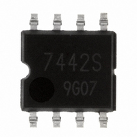
BU7442SF-E2 Rohm Semiconductor, BU7442SF-E2 Datasheet - Page 2

BU7442SF-E2
Manufacturer Part Number
BU7442SF-E2
Description
IC OPAMP 1.7-5.5V GRD SENSE 8SOP
Manufacturer
Rohm Semiconductor
Datasheet
1.BU7461G-TR.pdf
(37 pages)
Specifications of BU7442SF-E2
Amplifier Type
General Purpose
Number Of Circuits
2
Slew Rate
0.3 V/µs
Gain Bandwidth Product
600kHz
Current - Input Bias
1pA
Voltage - Input Offset
1000µV
Current - Supply
100µA
Current - Output / Channel
10mA
Voltage - Supply, Single/dual (±)
1.7 V ~ 5.5 V
Operating Temperature
-40°C ~ 105°C
Mounting Type
Surface Mount
Package / Case
8-SOP
Number Of Channels
2
Common Mode Rejection Ratio (min)
45 dB
Input Offset Voltage
6 mV
Input Bias Current (max)
1 pA
Output Current (typ)
6 mA, 10 mA
Operating Supply Voltage
1.7 V to 5.5 V
Supply Current
0.24 mA
Maximum Power Dissipation
620 mW
Maximum Operating Temperature
+ 105 C
Minimum Operating Temperature
- 40 C
Maximum Dual Supply Voltage
+/- 2.75 V
Minimum Dual Supply Voltage
+/- 0.85 V
Mounting Style
SMD/SMT
Shutdown
No
Supply Voltage (max)
5.5 V
Supply Voltage (min)
1.7 V
Technology
CMOS
Voltage Gain Db
95 dB
Lead Free Status / RoHS Status
Lead free / RoHS Compliant
Output Type
-
-3db Bandwidth
-
Lead Free Status / Rohs Status
Lead free / RoHS Compliant
Other names
BU7442SF-E2TR
Available stocks
Company
Part Number
Manufacturer
Quantity
Price
Company:
Part Number:
BU7442SF-E2
Manufacturer:
Rohm
Quantity:
8 000
BU7261/BU7261S family, BU7241/BU7241S family, BU7295/BU7295S family, BU7275/BU7275S family
BU7262/BU7262S family, BU7242/BU7242S family, BU7264/BU7264S family, BU7244/BU7244S family
●Pin Assignments
●Absolute maximum rating (Ta=25[℃])
© 2010 ROHM Co., Ltd. All rights reserved.
www.rohm.com
Input-output Full Swing
Supply Voltage
Differential Input Voltage
Input Common-mode Voltage Range
Operating Temperature
Storage Temperature
Maximum Junction Temperature
Note: Absolute maximum rating item indicates the condition which must not be exceeded.
(*1)
VSS
IN+
IN-
SSOP5
Application of voltage in excess of absolute maximum rating or use out absolute maximum rated temperature environment
may cause deterioration of characteristics.
The voltage difference between inverting input and non-inverting input is the differential input voltage.
Then input terminal voltage is set to more than VSS.
1
2
3
Input type
+
-
Parameter
HVSOF5
5
4
VDD
OUT
(*1)
BU7261G
BU7261SG
BU7241G
BU7241SG
SSOP5
SOP8
VDD-VSS
OUT1
BU7275HFV
BU7275SHFV
BU7295HFV
BU7295SHFV
Symbol
IN1+
VSS
Tjmax
IN1-
Vicm
Topr
Tstg
HVSOF5
Vid
1
2
3
4
MSOP8
BU7261G, BU7241G,
BU7262F/FVM/NUX
BU7242F/FVM/NUX
BU7264F, BU7244F
BU7295HFV, BU7275HFV
CH1
-
+
2/36
+
CH2
BU7262F
BU7262SF
BU7242F
BU7242SF
-
SOP8
-40 ~
8
7
6
5
VSON008X2030
VDD
OUT2
IN2-
IN2+
+
Package
85
(VSS-0.3)(VDD
VSON008X2030
BU7262NUX
BU7262SNUX
BU7242NUX
BU7242SNUX
VDD-VSS
-55 ~
+
+
125
Ratings
7
+
BU7261SG, BU7241SG,
BU7262SF/FVM/NUX
BU7242SF/FVM/NUX
BU7264SF, BU7244SF
BU7295SHFV, BU7275SHFV
125
OUT1
OUT2
IN1+
VDD
IN2+
IN1-
IN2-
+
0.3)
BU7262FVM
BU7262SFVM
BU7242FVM
BU7242SFVM
1
2
4
6
7
3
5
MSOP8
-40 ~
-
CH2
CH1
-
+
+
SOP14
+
105
Technical Note
2010.12 - Rev.A
+
+
CH4
CH3
BU7264F
BU7264SF
BU7244F
BU7244SF
-
-
SOP14
14
10
13
12
11
9
8
IN4+
VSS
OUT4
IN4-
IN3+
IN3-
OUT3
Unit
℃
℃
℃
V
V
V


