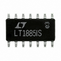
LT1885IS#PBF Linear Technology, LT1885IS#PBF Datasheet - Page 9

LT1885IS#PBF
Manufacturer Part Number
LT1885IS#PBF
Description
IC OPAMP QUAD R-R PICO/IN 14SOIC
Manufacturer
Linear Technology
Datasheet
1.LT1884CS8PBF.pdf
(12 pages)
Specifications of LT1885IS#PBF
Amplifier Type
General Purpose
Number Of Circuits
4
Output Type
Rail-to-Rail
Slew Rate
1 V/µs
Gain Bandwidth Product
2.2MHz
Current - Input Bias
150pA
Voltage - Input Offset
30µV
Current - Supply
850µA
Current - Output / Channel
50mA
Voltage - Supply, Single/dual (±)
2.7 V ~ 36 V, ±1.35 V ~ 18 V
Operating Temperature
-40°C ~ 85°C
Mounting Type
Surface Mount
Package / Case
14-SOIC (3.9mm Width), 14-SOL
Lead Free Status / RoHS Status
Lead free / RoHS Compliant
-3db Bandwidth
-
Available stocks
Company
Part Number
Manufacturer
Quantity
Price
APPLICATIO S I FOR ATIO
The LT1884/LT1885 dual op amp features exceptional
input precision with rail-to-rail output swing. Slew rate
and small-signal bandwidth are superior to other amplifi-
ers with comparable input precision. These characteris-
tics make the LT1884/LT1885 a convenient choice for
precision low voltage systems and for improved AC per-
formance in higher voltage precision systems. Maintain-
ing the advantage of the precision inherent in the amplifier
depends upon proper applications circuit design and
board layout.
Preserving Input Precision
Preserving the input voltage accuracy of the LT1884/
LT1885 requires that the applications circuit and PC board
layout do not introduce errors comparable to or greater
than the 30 V offset. Temperature differentials across the
input connections can generate thermocouple voltages of
10s of microvolts. PC board layouts should keep connec-
tions to the amplifier’s input pins close together and away
from heat dissipating components. Air currents across the
board can also generate temperature differentials.
The extremely low input bias currents, 100pA, allow high
accuracy to be maintained with high impedance sources
and feedback networks. The LT1884/LT1885’s low input
bias currents are obtained by using a cancellation circuit
on-chip. This causes the resulting I
uncorrelated, as implied by the I
comparable to the I
the input resistances in each input lead, as is commonly
recommended with most amplifiers. The impedance at
either input should be kept as small as possible to mini-
mize total circuit error.
PC board layout is important to ensure that leakage
currents do not corrupt the low I
high precision, high impedance circuits, the input pins
should be surrounded by a guard ring of PC board
BIAS
U
. The user should not try to balance
U
BIAS
OS
W
BIAS
specification being
of the amplifier. In
+
and I
BIAS
U
–
to be
interconnect, with the guard driven to the same common
mode voltage as the amplifier inputs.
Input Common Mode Range
The LT1884/LT1885 output is able to swing close to each
power supply rail, but the input stage is limited to operat-
ing between V
common mode range will cause the gain to drop to zero;
however, no gain reversal will occur.
Input Protection
The inverting and noninverting input pins of the LT1884/
LT1885 have limited on-chip protection. ESD protection is
provided to prevent damage during handling. The input
transistors have voltage clamping and limiting resistors to
protect against input differentials up to 10V. Short tran-
sients above this level will also be tolerated. If the input
pins may be subject to a sustained differential voltage
above 10V, external limiting resistors should be used to
prevent damage to the amplifier. A 1k resistor in each input
lead will provide protection against a 30V differential
voltage.
Capacitive Loads
The LT1884/LT1885 can drive capacitive loads up to
300pF when configured for unity gain. The capacitive load
driving capability increases as the amplifier is used in
higher gain configurations. Capacitive load driving may
also be increased by decoupling the capacitance from the
output with a small resistance.
Input Bias Currents
While it may be tempting to seek out a JFET amplifier for
low input bias current, remember that bipolar devices
improve with temperature while JFETs degrade.
EE
+ 0.8V and V
LT1884/LT1885
CC
– 0.9V. Exceeding this
9


