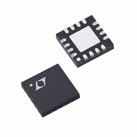
LT6402CUD-20#PBF Linear Technology, LT6402CUD-20#PBF Datasheet - Page 9

LT6402CUD-20#PBF
Manufacturer Part Number
LT6402CUD-20#PBF
Description
IC DIFF AMP/ADC DRVR 16-QFN
Manufacturer
Linear Technology
Datasheet
1.LT6402CUD-20PBF.pdf
(16 pages)
Specifications of LT6402CUD-20#PBF
Amplifier Type
Differential
Number Of Circuits
2
Output Type
Differential
Slew Rate
400 V/µs
-3db Bandwidth
300MHz
Current - Input Bias
5µA
Voltage - Input Offset
1000µV
Current - Supply
30mA
Current - Output / Channel
35mA
Voltage - Supply, Single/dual (±)
4 V ~ 5.5 V, ±2 V ~ 2.5 V
Operating Temperature
0°C ~ 70°C
Mounting Type
Surface Mount
Package / Case
16-WQFN Exposed Pad
No. Of Amplifiers
1
Input Offset Voltage
6.5mV
Gain Db Max
20dB
Bandwidth
300MHz
Supply Voltage Range
4V To 5.5V
Supply Current
30mA
Amplifier Case Style
QFN
Rohs Compliant
Yes
Lead Free Status / RoHS Status
Lead free / RoHS Compliant
Gain Bandwidth Product
-
Available stocks
Company
Part Number
Manufacturer
Quantity
Price
BLOCK DIAGRA
PI FU CTIO S
V
voltage. Without additional biasing, both inputs bias to
this voltage as well. This input is high impedance.
V
(Normally Tied to 5V). All three pins must be tied to the
same voltage. Bypass each pin with 1000pF and 0.1µF
capacitors as close to the package as possible. Split
supplies are possible as long as the voltage between V
and V
V
(Normally Tied to Ground). All three pins must be tied to
the same voltage. Split supplies are possible as long as
the voltage between V
not tied to ground, bypass each pin with 1000pF and 0.1µF
capacitors as close to the package as possible.
+OUT, –OUT (Pins 5, 8): Outputs (Unfi ltered). These
pins are high bandwidth, low-impedance outputs. The DC
output voltage at these pins is set to the voltage applied
at V
OCM
CCA
EEA
U
OCM
, V
, V
EE
(Pin 2): This pin sets the output common mode
EEB
CCB
.
is 5V.
U
, V
, V
EEC
CCC
(Pins 4, 9, 12): Negative Power Supply
(Pins 3, 10, 1): Positive Power Supply
U
CC
–INA
–INB
+INA
+INB
and V
W
14
13
16
15
EE
3
is 5V. If these pins are
V
CCA
100Ω
100Ω
100Ω
100Ω
500Ω
500Ω
10
V
CCB
1
–
+
+
–
V
CCC
A
B
500Ω
500Ω
V
V
V
V
CCA
CCB
EEA
EEB
CC
BIAS
11
V
V
ENABLE
CCC
EEC
+OUTFILTERED, –OUTFILTERED (Pins 6, 7): Filtered
Outputs. These pins add a series 50Ω resistor from the
unfi ltered outputs and three 14pF capacitors. Each output
has 14pF to V
(See the Block Diagram). This fi lter has a –3dB bandwidth
of 75MHz.
⎯ E ⎯ N ⎯ A ⎯ B ⎯ L ⎯ E (Pin 11): This pin is a TTL logic input referenced
to the V
typically 30mA of supply current. If high, the LT6402 is
disabled and draws typically 250µA.
+INA, +INB (Pins 15, 16): Positive Inputs. These pins are
normally tied together. These inputs may be DC- or AC-
coupled. If the inputs are AC-coupled, they will self-bias
to the voltage applied to the V
–INA, –INB (Pins 14, 13): Negative Inputs. These pins are
normally tied together. These inputs may be DC- or AC-
coupled. If the inputs are AC-coupled, they will self-bias
to the voltage applied to the V
Exposed Pad (Pin 17): Tie the pad to V
supplies are used, DO NOT tie the pad to ground.
C
+
–
4
V
EEA
EEC
9
pin. If low, the LT6402 is enabled and draws
14pF
14pF
14pF
50Ω
50Ω
V
EE
EEB
V
V
, plus an additional 14pF between each pin
EEA
EEB
12
V
EEC
5
6
2
7
8
+OUT
+OUTFILTERED
V
–OUTFILTERED
–OUT
6402 BD
OCM
OCM
OCM
pin.
pin.
LT6402-20
EEC
(Pin 12). If split
640220fa
9


