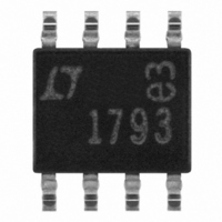
LT1793CS8#PBF Linear Technology, LT1793CS8#PBF Datasheet - Page 9

LT1793CS8#PBF
Manufacturer Part Number
LT1793CS8#PBF
Description
IC PREC OPAMP JFET LOWNOIS 8SOIC
Manufacturer
Linear Technology
Datasheet
1.LT1793CS8PBF.pdf
(12 pages)
Specifications of LT1793CS8#PBF
Amplifier Type
J-FET
Number Of Circuits
1
Slew Rate
3.4 V/µs
Gain Bandwidth Product
4.2MHz
Current - Input Bias
4pA
Voltage - Input Offset
250µV
Current - Supply
4.2mA
Voltage - Supply, Single/dual (±)
±4.5 V ~ 20 V
Operating Temperature
0°C ~ 70°C
Mounting Type
Surface Mount
Package / Case
8-SOIC (3.9mm Width)
Lead Free Status / RoHS Status
Lead free / RoHS Compliant
Output Type
-
Current - Output / Channel
-
-3db Bandwidth
-
Available stocks
Company
Part Number
Manufacturer
Quantity
Price
A
resulting in a change in voltage dV, which is equal to dQ/C
The gain therefore is C
equal the transducer capacitance plus the input capaci-
tance of the LT1793 and R
In the noninverting mode example, the transducer current
is converted to a change in voltage by the transducer
capacitance, C
LT1793 with a gain of 1 + R1/R2. A DC path is provided by
R
nal resistor. Since R
tude greater than the parallel combination of R1 and R2, R
is added to balance the DC offset caused by the noninvert-
ing input bias current and R
although small at room temperature, can create significant
errors at higher temperature, especially with transducer
resistances of up to 1000M or more. The optimum value
S
PPLICATI
, which is either the transducer impedance or an exter-
S
. This voltage is then buffered by the
O
Input: 5.2V Sine Wave
U
S
Figure 5. Voltage Follower with Input Exceeding the Common Mode Range (V
is usually several orders of magni-
S
F
/C
I FOR ATIO
S
U
F
. For unity-gain, the C
should equal R
S
. The input bias currents,
W
LT1793 F05a
S
.
U
F
should
F
B
.
for R
to the current noise (2qI
results in R
capacitor C
the op amp input capacitance and R
Reduced Power Supply Operation
To take full advantage of a wide input common mode range,
the LT1793 was designed to eliminate phase reversal.
Referring to the photographs in Figure 5, the LT1793 is
shown operating in the follower mode (A
supplies with the input swinging 5.2V. The output of the
LT1793 clips cleanly and recovers with no phase reversal.
This has the benefit of preventing lockup in servo systems
and minimizing distortion components.
B
is determined by equating the thermal noise (4kTR
B
B
, is used to cancel the phase shift caused by
= R
S
= 2V
T
LT1793 Output
/I
B
B
(V
) times R
S
T
= 5V)
= 26mV at 25 C). A parallel
B
.
S
2
. Solving for R
LT1793 F05b
V
= 1) at 5V
LT1793
9
S
S
)


