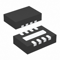
LTC6102CDD-1#PBF Linear Technology, LTC6102CDD-1#PBF Datasheet - Page 14

LTC6102CDD-1#PBF
Manufacturer Part Number
LTC6102CDD-1#PBF
Description
IC AMP CURRENT SENSE 8-DFN
Manufacturer
Linear Technology
Datasheet
1.LTC6102CDDPBF.pdf
(26 pages)
Specifications of LTC6102CDD-1#PBF
Amplifier Type
Current Sense
Number Of Circuits
1
Gain Bandwidth Product
200kHz
Current - Input Bias
60pA
Voltage - Input Offset
3µV
Current - Supply
420µA
Current - Output / Channel
1mA
Voltage - Supply, Single/dual (±)
4 V ~ 60 V
Operating Temperature
0°C ~ 70°C
Mounting Type
Surface Mount
Package / Case
8-DFN
No. Of Amplifiers
1
Input Bias Current
3nA
Output Current Per Channel
1mA
Input Offset Voltage
10µV
Bandwidth
200kHz
Supply Voltage Range
4V To 60V
Supply Current
650µA
Rohs Compliant
Yes
Lead Free Status / RoHS Status
Lead free / RoHS Compliant
Output Type
-
-3db Bandwidth
-
Slew Rate
-
Available stocks
Company
Part Number
Manufacturer
Quantity
Price
APPLICATIONS INFORMATION
LTC6102
LTC6102-1/LTC6102HV
the largest expected sense voltage gives I
the maximum output dynamic range is available. Output
dynamic range is limited by both the maximum allowed
output current (Note 1) and the maximum allowed output
voltage, as well as the minimum practical output signal. If
less dynamic range is required, then R
accordingly, reducing the output current and power dis-
sipation. If small sense currents must be resolved ac-
curately in a system that has very wide dynamic range, a
smaller R
another way, such as with a Schottky diode across R
(Figure 3). This will reduce the high current measurement
accuracy by limiting the result, while increasing the low
current measurement resolution. This approach can be
helpful in cases where occasional large burst currents
may be ignored.
Care should be taken when designing the PC board lay-
out for R
interconnect impedances will increase the effective R
value, causing a gain error. It is important to note that the
large temperature drift of copper resistance will cause a
change in gain over temperature if proper care is not taken
to reduce this effect.
To further limit the effect of trace resistance on gain,
maximizing the accuracy of these circuits, the LTC6102 has
been designed with a Kelvin input. The inverting terminal
(–INS) is separate from the feedback path (–INF). During
operation, these two pins must be connected together.
The design of the LTC6102 is such that current into –INS
is input bias current only, which is typically 60pA at 25°C.
Almost all of the current from R
14
Figure 3. Shunt Diode Limits Maximum Input Voltage to Allow
Better Low Input Resolution Without Overranging
IN
IN
, especially for small R
may be used if the max current is limited in
R
SENSE
LOAD
V
+
6102 F03
IN
D
SENSE
fl ows into –INF , through
IN
values. All trace and
IN
can be increased
OUT
= 1mA, then
SENSE
IN
the LTC6102, and into R
minimize gain error, –INS should be routed in a separate
path from –INF to a point as close to R
addition, the higher potential terminal of R
connected directly to the positive terminal of R
any input voltage source). For the highest accuracy, R
should be a four-terminal resistor if it is less than 10Ω.
Selection of External Output Resistor, R
The output resistor, R
rent is converted to voltage. V
In choosing an output resistor, the max output voltage
must fi rst be considered. If the circuit that is driven by the
output does not have a limited input voltage, then R
must be chosen such that the max output voltage does
not exceed the LTC6102 max output voltage rating. If the
following circuit is a buffer or ADC with limited input range,
then R
than the allowed maximum input range of this circuit.
In addition, the output impedance is determined by R
the circuit to be driven has high enough input impedance,
then almost any output impedance will be acceptable.
However, if the driven circuit has relatively low input imped-
ance, or draws spikes of current, such as an ADC might
do, then a lower R
preserve the accuracy of the output. As an example, if the
input impedance of the driven circuit is 100 times R
then the accuracy of V
Error Sources
The current sense system uses an amplifi er and resistors
to apply gain and level shift the result. The output is then
dependent on the characteristics of the amplifi er, such as
gain and input offset, as well as resistor matching.
V
OUT
OUT
=
=
must be chosen so that I
I
I I
OUT
OUT
•
•
R
R
R
OUT
OUT
OUT
OUT
OUT
OUT
+
•
value may be required in order to
•
100
R
101
R
OUT
, determines how the output cur-
IN DRIVEN
IN DRIVEN
will be reduced by 1% since:
(
(
=
via the OUT pin. In order to
OUT
0 99
.
is simply I
OUT(MAX)
)
)
•
I
OUT
IN
OUT
•
as possible. In
R
• R
IN
OUT
OUT
should be
OUT
SENSE
• R
is less
OUT
OUT
OUT
6102fd
OUT
(or
. If
IN
.
,


