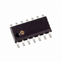
MCP6034-E/SL Microchip Technology, MCP6034-E/SL Datasheet - Page 15

MCP6034-E/SL
Manufacturer Part Number
MCP6034-E/SL
Description
IC OPAMP QUAD 1.8V 14SOIC
Manufacturer
Microchip Technology
Specifications of MCP6034-E/SL
Slew Rate
0.004 V/µs
Package / Case
14-SOIC (3.9mm Width), 14-SOL
Amplifier Type
General Purpose
Number Of Circuits
4
Output Type
Rail-to-Rail
Gain Bandwidth Product
10kHz
Current - Input Bias
1pA
Voltage - Input Offset
150µV
Current - Supply
0.9µA
Current - Output / Channel
23mA
Voltage - Supply, Single/dual (±)
1.8 V ~ 5.5 V
Operating Temperature
-40°C ~ 125°C
Mounting Type
Surface Mount
Number Of Channels
4
Common Mode Rejection Ratio (min)
70 dB
Input Offset Voltage
0.15 mV
Input Bias Current (max)
100 pA
Operating Supply Voltage
3 V, 5 V
Supply Current
0.0054 mA
Maximum Operating Temperature
+ 125 C
Minimum Operating Temperature
- 40 C
Mounting Style
SMD/SMT
Shutdown
No
Supply Voltage (max)
5.5 V
Supply Voltage (min)
1.8 V
Technology
CMOS
Voltage Gain Db
115 dB
Lead Free Status / RoHS Status
Lead free / RoHS Compliant
-3db Bandwidth
-
Lead Free Status / Rohs Status
Lead free / RoHS Compliant
Available stocks
Company
Part Number
Manufacturer
Quantity
Price
Company:
Part Number:
MCP6034-E/SL
Manufacturer:
Microchip
Quantity:
6 366
Part Number:
MCP6034-E/SL
Manufacturer:
MICROCHIP/微芯
Quantity:
20 000
4.2
The output voltage range of the MCP6031/2/3/4 op
amps is V
(maximum) when R
and V
more information.
4.3
The MCP6031/2/3/4 op amp family has outstanding
quiescent current, which supports battery-powered
applications. There is minimal quiescent current glitch-
ing when Chip Select (CS) is raised or lowered. This
prevents excessive current draw, and reduced battery
life, when the part is turned off or on.
Heavy resistive loads at the output can cause exces-
sive battery drain. Driving a DC voltage of 2.5V across
a 100 kΩ load resistor will cause the supply current to
increase by 25 µA, depleting the battery 28 times as
fast as I
High frequency signals (fast edge rate) across capaci-
tive loads will also significantly increase supply current.
For instance, a 0.1 µF capacitor at the output presents
an AC impedance of 15.9 kΩ (1/2πfC) to a 100 Hz
sinewave. It can be shown that the average power
drawn from the battery by a 5.0 V
(1.77 V
EQUATION 4-1:
This will drain the battery about 12 times as fast as I
alone.
4.4
Driving large capacitive loads can cause stability
problems for voltage feedback op amps. As the load
capacitance increases, the feedback loop’s phase
margin decreases and the closed-loop bandwidth is
reduced. This produces gain peaking in the frequency
response, with overshoot and ringing in the step
response. While a unity-gain buffer (G = +1) is the most
sensitive to capacitive loads, all gains show the same
general behavior.
When driving large capacitive loads with these op
amps (e.g., > 100 pF when G = +1), a small series
resistor at the output (R
feedback loop’s phase margin (stability) by making the
output load resistive at higher frequencies. The
bandwidth will be generally lower than the bandwidth
with no capacitance load.
© 2008 Microchip Technology Inc.
P
Supply
DD
rms
Q
Rail-to-Rail Output
Output Loads and Battery Life
Capacitive Loads
= 5.5V. Refer to
(0.9 µA, typical) alone.
= (V
), under these conditions, is
= (5V)(0.9 µA + 5.0V
= 4.5 µW + 50 µW
SS
+ 10 mV (minimum) and V
DD
- V
SS
L
) (I
= 50 kΩ is connected to V
ISO
Q
+ V
Figures 2-25
in
Figure
L(p-p)
p-p
·
100Hz
f C
4-3) improves the
L
)
p-p
and
·
DD
0.1µF)
sinewave
– 10 mV
2-26
DD
for
/2
Q
FIGURE 4-3:
stabilizes large capacitive loads.
Figure 4-4
different capacitive loads and gains. The x-axis is the
normalized load capacitance (C
circuit's noise gain. For non-inverting gains, G
Signal Gain are equal. For inverting gains, G
1+|Signal Gain| (e.g., -1 V/V gives G
FIGURE 4-4:
for Capacitive Loads.
After selecting R
resulting frequency response peaking and step
response overshoot. Modify R
response is reasonable. Bench evaluation and simula-
tions with the MCP6031/2/3/4 SPICE macro model are
very helpful.
4.5
The MCP6033 is a single op amp with Chip Select
(CS). When CS is pulled high, the supply current drops
to 0.4 nA (typical) and flows through the CS pin to V
When this happens, the amplifier output is put into a
high impedance state. By pulling CS low, the amplifier
is enabled. If the CS pin is left floating, the amplifier will
not operate properly.
voltage and supply current response to a CS pulse.
V
IN
1000000
100000
10000
100k
1000
MCP6033 Chip Select
10k
1M
1k
1.E-11
gives recommended R
10p
+
–
MCP603X
Normalized Load Capacitance; C
MCP6031/2/3/4
ISO
1.E-10
100p
for your circuit, double-check the
Output resistor, R
Recommended R
G
1 V/V
2 V/V
≥ 5 V/V
Figure 1-1
N
:
1.E-09
1n
R
L
ISO
1.E-08
ISO
/G
10n
C
N
’s value until the
shows the output
), where G
N
DS22041B-page 15
L
ISO
= +2 V/V).
1.E-07
100n
ISO
ISO
L
/G
values for
N
N
(F)
V
values
1.E-06
and the
N
OUT
1µ
is the
N
SS
is
.


