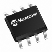
MCP6S92-E/MS Microchip Technology, MCP6S92-E/MS Datasheet - Page 21

MCP6S92-E/MS
Manufacturer Part Number
MCP6S92-E/MS
Description
IC PGA 2CH R-R I/O SPI 8MSOP
Manufacturer
Microchip Technology
Datasheet
1.MCP6S91-ESN.pdf
(40 pages)
Specifications of MCP6S92-E/MS
Amplifier Type
Programmable Gain
Number Of Circuits
2
Output Type
Rail-to-Rail
Slew Rate
22 V/µs
-3db Bandwidth
18MHz
Current - Input Bias
1pA
Voltage - Input Offset
400µV
Current - Supply
1mA
Current - Output / Channel
25mA
Voltage - Supply, Single/dual (±)
2.5 V ~ 5.5 V
Operating Temperature
-40°C ~ 125°C
Mounting Type
Surface Mount
Package / Case
8-MSOP, Micro8™, 8-uMAX, 8-uSOP,
For Use With
MCP6SX2DM-PCTLPD - BOARD DAUGHTER PICTAIL MCP6SX2
Lead Free Status / RoHS Status
Lead free / RoHS Compliant
Gain Bandwidth Product
-
Other names
MCP6S92-E/MSR
MCP6S92-E/MSR
MCP6S92-E/MSR
Available stocks
Company
Part Number
Manufacturer
Quantity
Price
Company:
Part Number:
MCP6S92-E/MS
Manufacturer:
Microchip
Quantity:
2 617
5.0
The MCP6S91/2/3 PGAs use a standard SPI
compatible serial interface to receive instructions from
a controller. This interface is configured to allow daisy-
chaining with other SPI devices.
5.1
Chip Select (CS) toggles low to initiate communica-
tion with these devices. The first byte of each SI word
(two bytes long) is the instruction byte, which goes
into the Instruction register. The Instruction register
points the second byte to its destination. In a typical
application, CS is raised after one word (16 bits) to
implement the desired changes. Section 5.3 “Daisy-
FIGURE 5-1:
FIGURE 5-2:
2004 Microchip Technology Inc.
SCK
SO
CS
SCK
SI
SO
CS
SI
DIGITAL FUNCTIONS
SPI Timing
(first 16 bits out are always zeros)
(first 16 bits out are always zeros)
Serial Bus Sequence for the PGA; SPI™ 0,0 Mode (see Figure 1-4).
Serial Bus Sequence for the PGA; SPI™ 1,1 Mode (see Figure 1-5).
1
1
2
2
Instruction Byte
Instruction Byte
3
3
4
4
5
5
6
6
7
7
8
8
Chain Configuration”, covers applications using
multiple 16-bit words. SO goes low after CS goes
high; it has a push-pull output that does not go into a
high-Z state.
The MCP6S91/2/3 devices operate in SPI modes 0,0
and 1,1. In 0,0 mode, the clock idles in the low state
(Figure 5-1). In 1,1 mode, the clock idles in the high
state (Figure 5-2). In both modes, SI data is loaded into
the PGA on the rising edge of SCK, while SO data is
clocked out on the falling edge of SCK. In 0,0 mode, the
falling edge of CS also acts as the first falling edge of
SCK (see Figure 5-1). There must be multiples of 16
clocks (SCK) while CS is low or commands will abort
(see Section 5.3 “Daisy-Chain Configuration”).
9
9
10
10
11
11
Data Byte
Data Byte
12
12
13
MCP6S91/2/3
13
14
14
15
15
16
16
DS21908A-page 21


