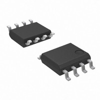
AP358SG-13 Diodes Inc, AP358SG-13 Datasheet - Page 8

AP358SG-13
Manufacturer Part Number
AP358SG-13
Description
IC OPAMP DUAL LOW POWER 8-SOIC
Manufacturer
Diodes Inc
Datasheet
1.AP358SG-13.pdf
(16 pages)
Specifications of AP358SG-13
Amplifier Type
General Purpose
Number Of Circuits
2
Gain Bandwidth Product
1MHz
Current - Input Bias
45nA
Voltage - Input Offset
2000µV
Current - Supply
1mA
Current - Output / Channel
40mA
Voltage - Supply, Single/dual (±)
3 V ~ 32 V, ±1.5 V ~ 16 V
Operating Temperature
0°C ~ 70°C
Mounting Type
Surface Mount
Package / Case
8-SOIC (3.9mm Width)
Number Of Channels
2
Common Mode Rejection Ratio (min)
65 dB
Input Offset Voltage
7 mV
Input Bias Current (max)
250 nA
Output Current (typ)
40 mA
Operating Supply Voltage
32 V
Supply Current
1.2 mA
Maximum Power Dissipation
600 mW
Maximum Operating Temperature
+ 70 C
Minimum Operating Temperature
0 C
Dual Supply Voltage
+/- 3 V, +/- 5 V, +/- 9 V
Maximum Dual Supply Voltage
+/- 16 V
Minimum Dual Supply Voltage
+/- 1.5 V
Mounting Style
SMD/SMT
Shutdown
No
Supply Voltage (max)
32 V
Supply Voltage (min)
3 V
Voltage Gain Db
100 dB
Lead Free Status / RoHS Status
Lead free / RoHS Compliant
Output Type
-
-3db Bandwidth
-
Slew Rate
-
Lead Free Status / Rohs Status
Lead free / RoHS Compliant
Other names
AP358SGDITR
Available stocks
Company
Part Number
Manufacturer
Quantity
Price
Company:
Part Number:
AP358SG-13
Manufacturer:
DIODES
Quantity:
1 625
Part Number:
AP358SG-13
Manufacturer:
DIODES/美台
Quantity:
20 000
Company:
Part Number:
AP358SG-13-89
Manufacturer:
DIODES
Quantity:
2 869
Absolute Maximum Ratings
Notes:
AP358
Document number: DS31007 Rev. 6 - 2
Symbol
V
T
T
V
P
CC
OP
ST
IN
D
2. For operating at high temperatures, the AP358 must be derated based on a +125°C maximum junction temperature and a
3. Short circuits from the output to V
4. This input current will only exist when the voltage at any of the input leads is driven negative. It is due to the collector-base
thermal resistance of 120°C/W for DIP and 189°C/W for Small Outline package, which applies for the device soldered in a
printed circuit board, operating in a still air ambient. The dissipation is the total of both amplifiers—use external resistors,
where possible, to allow the amplifier to saturate or to reduce the power which is dissipated in the integrated circuit.
voltage in excess of +15V, continuous short-circuits can exceed the power dissipation ratings and cause eventual
destruction. Destructive dissipation can result from simultaneous shorts on all amplifiers.
voltages of the op amps to go to the V
driven negative. This is not destructive and normal output states will re-establish when the input voltage, which was
negative, again returns to a value greater than -0.3V (at 25°C).
to ground, the maximum output current is approximately 40mA independent of the magnitude of V
diode action, there is also lateral NPN parasitic transistor action on the IC chip. This transistor action can cause the output
junction of the input PNP transistors becoming forward biased and thereby acting as input diode clamps. In addition to this
Supply voltage
Differential Input Voltage
Input Voltage
Power Dissipation (Note 2)
Output Short-Circuit to GND
(One Amplifier) (Note 3)
Operating Temperature Range
Storage Temperature Range
+
can cause excessive heating and eventual destruction. When considering short circuits
Parameter
+
voltage level (or to ground for a large overdrive) for the time duration that an input is
V
Input Current (V
(Note 4)
+
< 15V and T
www.diodes.com
LOW POWER DUAL OPERATIONAL AMPLIFIERS
8 of 16
A
IN
=25
< -0.3V)
o
C
Continuous
-65 to +150
-0.3 to +32
0 to +70
Rating
600
32
32
40
+
. At values of supply
© Diodes Incorporated
AP358
Unit
mW
mA
July 2010
o
o
V
V
V
C
C


