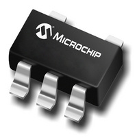
MCP6001T-I/LT Microchip Technology, MCP6001T-I/LT Datasheet - Page 10

MCP6001T-I/LT
Manufacturer Part Number
MCP6001T-I/LT
Description
IC OPAMP 1.8V 1MHZ SINGLE SC70-5
Manufacturer
Microchip Technology
Specifications of MCP6001T-I/LT
Slew Rate
0.6 V/µs
Package / Case
SC-70-5, SC-88A, SOT-323-5, SOT-353, 5-TSSOP
Amplifier Type
General Purpose
Number Of Circuits
1
Output Type
Rail-to-Rail
Gain Bandwidth Product
1MHz
Current - Input Bias
1pA
Voltage - Input Offset
4500µV
Current - Supply
100µA
Current - Output / Channel
23mA
Voltage - Supply, Single/dual (±)
1.8 V ~ 6 V
Operating Temperature
-40°C ~ 85°C
Mounting Type
Surface Mount
Number Of Channels
1
Common Mode Rejection Ratio (min)
60 dB
Input Offset Voltage
4.5 mV
Input Bias Current (max)
19 pA
Operating Supply Voltage
3 V, 5 V
Maximum Operating Temperature
+ 85 C
Minimum Operating Temperature
- 40 C
Mounting Style
SMD/SMT
Shutdown
No
Supply Voltage (max)
6 V
Supply Voltage (min)
1.8 V
Technology
CMOS
Voltage Gain Db
112 dB
Lead Free Status / RoHS Status
Lead free / RoHS Compliant
For Use With
MCP6SX2DM-PCTLPD - BOARD DAUGHTER PICTAIL MCP6SX2
-3db Bandwidth
-
Lead Free Status / Rohs Status
Lead free / RoHS Compliant
Other names
MCP6001T-I/LT
MCP6001T-I/LTTR
MCP6001T-I/LTTR
Available stocks
Company
Part Number
Manufacturer
Quantity
Price
Company:
Part Number:
MCP6001T-I/LT
Manufacturer:
MICROCHIP
Quantity:
16 000
Company:
Part Number:
MCP6001T-I/LT
Manufacturer:
Microchip Technology
Quantity:
60 860
Part Number:
MCP6001T-I/LT
Manufacturer:
MICROCHIP/微芯
Quantity:
20 000
MCP6001/2/4
4.6
4.6.1
The rail-to-rail input and output capability of the
MCP6001/2/4 op amp is ideal for unity-gain buffer
applications. The low quiescent current and wide
bandwidth makes the device suitable for a buffer
configuration in an instrumentation amplifier circuit, as
shown in Figure 4-6.
FIGURE 4-6:
with Unity-Gain Buffer Inputs.
4.6.2
The MCP6001/2/4 op amp’s low input bias current
makes it possible for the designer to use larger resis-
tors and smaller capacitors for active low-pass filter
applications. However, as the resistance increases, the
noise generated also increases. Parasitic capacitances
and the large value resistors could also modify the fre-
quency response. These trade-offs need to be
considered when selecting circuit elements.
Usually, the op amp bandwidth is 100X the filter cutoff
frequency (or higher) for good performance. It is possi-
ble to have the op amp bandwidth 10X higher than the
cutoff frequency, thus having a design that is more
sensitive to component tolerances.
Figure 4-7 shows a second-order Butterworth filter with
100 kHz cutoff frequency and a gain of +1 V/V; the op
amp bandwidth is only 10X higher than the cutoff
frequency. The component values were selected using
Microchip’s FilterLab
DS21733E-page 10
V
V
IN1
IN2
Application Circuits
V
OUT
UNITY-GAIN BUFFER
ACTIVE LOW-PASS FILTER
MCP6002
MCP6002
+
–
+
–
1/2
1/2
=
V
®
IN2
software.
Instrumentation Amplifier
–
V
R
R
2
IN1
2
R
–
+
V
MCP6001
1
R
----- -
R
REF
1
2
R
+
1
V
REF
R
R
1
2
= 20 k
= 10 k
V
OUT
FIGURE 4-7:
Low- Pass Filter.
4.6.3
The MCP6001/2/4 op amp has a high input impedance,
rail-to-rail input/output and low input bias current, which
makes this device suitable for peak detector applica-
tions. Figure 4-8 shows a peak detector circuit with
clear and sample switches. The peak-detection cycle
uses a clock (CLK), as shown in Figure 4-8.
At the rising edge of CLK, Sample Switch closes to
begin sampling. The peak voltage stored on C
pled to C
end of the sample time (falling edge of Sample Signal),
Clear Signal goes high and closes the Clear Switch.
When the Clear Switch closes, C
R
time (falling edge of Clear Signal), op amp A begins to
store the peak value of V
t
In order to define t
determine the capacitor charging and discharging
period. The capacitor charging time is limited by the
amplifier source current, while the discharging time ( )
is defined using R
the input signal is sampled on C
the input voltage change frequency.
The op amp output current limit, and the size of the
storage capacitors (both C
ing limitations as the input voltage (V
Current through a capacitor is dependent on the size of
the capacitor and the rate of voltage change. From this
relationship, the rate of voltage change or the slew rate
can be determined. For example, with an op amp short-
circuit current of I
C
EQUATION 4-1:
DETECT
1
1
for a time defined by t
= 0.1 µF, then:
V
IN
14.3 k
.
2
for a sample time defined by t
PEAK DETECTOR
53.6 k
33 pF
dV
------------ -
1
SC
SAMP
dt
( = R
dV
------------ -
C1
dt
= 25 mA and a load capacitor of
C1
I
Active Second-Order
SC
=
2004 Microchip Technology Inc.
and t
CLEAR
IN
=
=
1
100 pF
1
250mV
=
C
on C
and C
I
------- -
-------------- -
0.1 F
25mA
C
1
SC
C
). t
CLEAR
1
1
. At the end of the clear
dV
------------ -
DETECT
1
1
MCP6002
+
–
dt
1
2
for a time defined by
and is dependent on
), could create slew-
C1
discharges through
s
, it is necessary to
is the time that
IN
SAMP
) increases.
1
V
is sam-
. At the
OUT


