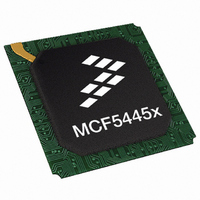
MCF54453VR266 Freescale Semiconductor, MCF54453VR266 Datasheet - Page 36

MCF54453VR266
Manufacturer Part Number
MCF54453VR266
Description
IC MPU 32BIT 266MHZ 360TEPBGA
Manufacturer
Freescale Semiconductor
Series
MCF5445xr
Datasheet
1.MCF54452CVR200.pdf
(48 pages)
Specifications of MCF54453VR266
Core Processor
Coldfire V4
Core Size
32-Bit
Speed
266MHz
Connectivity
I²C, SPI, SSI, UART/USART, USB OTG
Peripherals
DMA, WDT
Number Of I /o
132
Program Memory Type
ROMless
Ram Size
32K x 8
Voltage - Supply (vcc/vdd)
1.35 V ~ 3.6 V
Oscillator Type
Internal
Operating Temperature
0°C ~ 70°C
Package / Case
360-TEPBGA
Processor Series
MCF544x
Core
ColdFire V4
Data Bus Width
32 bit
Program Memory Size
16 KB
Data Ram Size
32 KB
Interface Type
I2C, SPI, SSI
Maximum Clock Frequency
66 MHz
Number Of Timers
8
Operating Supply Voltage
- 0.3 V to + 4 V
Maximum Operating Temperature
+ 70 C
Mounting Style
SMD/SMT
3rd Party Development Tools
JLINK-CF-BDM26, EWCF
Development Tools By Supplier
M54455EVB
Minimum Operating Temperature
0 C
On-chip Adc
16 bit, 16 Channel
On-chip Dac
16 bit, 16 Channel
For Use With
M54455EVB - BOARD EVAL FOR MCF5445X
Lead Free Status / RoHS Status
Lead free / RoHS Compliant
Eeprom Size
-
Program Memory Size
-
Data Converters
-
Lead Free Status / Rohs Status
Lead free / RoHS Compliant
Available stocks
Company
Part Number
Manufacturer
Quantity
Price
Company:
Part Number:
MCF54453VR266
Manufacturer:
Freescale Semiconductor
Quantity:
135
Electrical Characteristics
5.15
The ATA controller is compatible with the ATA/ATAPI-6 industry standard. Refer to the ATA/ATAPI-6 Specficiation and the
ATA controller chapter of the MCF54455 Reference Manual for timing diagrams of the various modes of operation.
The timings of the various ATA data transfer modes are determined by a set of timing equations described in the ATA section
of the MCF54455 Reference Manual. These timing equations must be fulfilled for the ATA host to meet timing.
provides implementation specific timing parameters necessary to complete the timing equations.
5.16
The DMA Serial Peripheral Interface (DSPI) provides a synchronous serial bus with master and slave operations. Many of the
transfer attributes are programmable.
DSPI chapter of the MCF54455 Reference Manual for information on the modified transfer formats used for communicating
with slower peripheral devices.
36
Master Mode
Slave Mode
Name
1
2
3
4
DS1
DS2
DS3
DS4
DS5
DS6
DS7
DS8
DS9
Name
These parameters are guaranteed by design and not testable.
All timings specified with a capacitive load of 40pF.
Applies to ATA_CS[1:0], ATA_DA[2:0], ATA_DIOR, ATA_DIOW, ATA_DMACK, ATA_DATA[15:0]
Applies to Ultra DMA data-in burst only
A1
A2
A3
A4
A5
A6
A7
ATA Interface Timing Specifications
DSPI Timing Specifications
DSPI_SCK Cycle Time
DSPI_SCK Duty Cycle
DSPI_PCSn to DSPI_SCK delay
DSPI_SCK to DSPI_PCSn delay
DSPI_SCK to DSPI_SOUT valid
DSPI_SCK to DSPI_SOUT invalid
DSPI_SIN to DSPI_SCK input setup
DSPI_SCK to DSPI_SIN input hold
DSPI_SCK to DSPI_SOUT valid
Setup time — ATA_IORDY to SYSCLK falling
Hold time — ATA_IORDY from SYSCLK falling
Setup time — ATA_DATA[15:0] to SYSCLK rising
Propagation delay — SYSCLK rising to all outputs
Output skew
Setup time — ATA_DATA[15:0] valid to ATA_IORDY
Hold time — ATA_IORDY to ATA_DATA[15:0] invalid
Characteristic
MCF5445x ColdFire
Table 26. DSPI Module AC Timing Specifications
Table 25. ATA Interface Timing Specifications
Characteristic
Table 26
provides DSPI timing characteristics for classic SPI timing modes. Refer to the
®
Microprocessor Data Sheet, Rev. 6
Symbol
t
t
t
SCK
CSC
ASC
—
—
—
—
—
—
(2 × t
(2 × t
(t
sck
Symbol
t
SKEW1
4 x t
t
t
t
I_DS
I_DH
t
t
SUI
t
CO
SU
SYS
SYS
÷ 2) - 2.0
HI
Min
—
—
-5
9
0
SYS
) - 1.5
) - 3.0
Min
4.0
3.0
4.0
2.0
3.5
—
—
1,2
(t
sck
1
÷ 2) + 2.0
Max
Max
10
—
—
—
—
—
—
7.0
1.5
5
—
—
—
—
—
Freescale Semiconductor
Unit
ns
ns
ns
ns
ns
ns
ns
Unit
ns
ns
ns
ns
ns
ns
ns
ns
ns
Notes
Table 25
3
3
4
4
Notes
2
3
4
5


