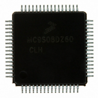
MC9S08DZ60CLH Freescale Semiconductor, MC9S08DZ60CLH Datasheet - Page 140

MC9S08DZ60CLH
Manufacturer Part Number
MC9S08DZ60CLH
Description
IC MCU 60K FLASH 4K RAM 64-LQFP
Manufacturer
Freescale Semiconductor
Series
HCS08r
Specifications of MC9S08DZ60CLH
Core Processor
HCS08
Core Size
8-Bit
Speed
40MHz
Connectivity
CAN, I²C, LIN, SCI, SPI
Peripherals
LVD, POR, PWM, WDT
Number Of I /o
53
Program Memory Size
60KB (60K x 8)
Program Memory Type
FLASH
Eeprom Size
2K x 8
Ram Size
4K x 8
Voltage - Supply (vcc/vdd)
2.7 V ~ 5.5 V
Data Converters
A/D 24x12b
Oscillator Type
External
Operating Temperature
-40°C ~ 85°C
Package / Case
64-LQFP
For Use With
DEMO9S08DZ60 - BOARD DEMOEVB9S08DZ60 - BOARD EVAL FOR 9S08DZ60
Lead Free Status / RoHS Status
Lead free / RoHS Compliant
Available stocks
Company
Part Number
Manufacturer
Quantity
Price
Company:
Part Number:
MC9S08DZ60CLH
Manufacturer:
FREESCALE
Quantity:
2 880
Company:
Part Number:
MC9S08DZ60CLH
Manufacturer:
Freescale Semiconductor
Quantity:
10 000
- Current page: 140 of 416
- Download datasheet (5Mb)
Chapter 8 Multi-Purpose Clock Generator (S08MCGV1)
8.3
8.3.1
140
IREFSTEN
IRCLKEN
IREFS
CLKS
Field
RDIV
7:6
5:3
2
1
0
Reset:
Register Definition
W
R
MCG Control Register 1 (MCGC1)
Clock Source Select — Selects the system clock source.
00
01
10
11
Reference Divider — Selects the amount to divide down the reference clock selected by the IREFS bit. If the
FLL is selected, the resulting frequency must be in the range 31.25 kHz to 39.0625 kHz. If the PLL is selected,
the resulting frequency must be in the range 1 MHz to 2 MHz.
000 Encoding 0 — Divides reference clock by 1 (reset default)
001 Encoding 1 — Divides reference clock by 2
010 Encoding 2 — Divides reference clock by 4
011 Encoding 3 — Divides reference clock by 8
100 Encoding 4 — Divides reference clock by 16
101 Encoding 5 — Divides reference clock by 32
110 Encoding 6 — Divides reference clock by 64
111 Encoding 7 — Divides reference clock by 128
Internal Reference Select — Selects the reference clock source.
1 Internal reference clock selected
0 External reference clock selected
Internal Reference Clock Enable — Enables the internal reference clock for use as MCGIRCLK.
1 MCGIRCLK active
0 MCGIRCLK inactive
Internal Reference Stop Enable — Controls whether or not the internal reference clock remains enabled when
the MCG enters stop mode.
1 Internal reference clock stays enabled in stop if IRCLKEN is set or if MCG is in FEI, FBI, or BLPI mode before
0 Internal reference clock is disabled in stop
entering stop
Encoding 0 — Output of FLL or PLL is selected.
Encoding 1 — Internal reference clock is selected.
Encoding 2 — External reference clock is selected.
Encoding 3 — Reserved, defaults to 00.
7
0
CLKS
Table 8-1. MCG Control Register 1 Field Descriptions
0
6
Figure 8-3. MCG Control Register 1 (MCGC1)
MC9S08DZ60 Series Data Sheet, Rev. 4
0
5
RDIV
0
4
Description
0
3
IREFS
1
2
IRCLKEN
Freescale Semiconductor
0
1
IREFSTEN
0
0
Related parts for MC9S08DZ60CLH
Image
Part Number
Description
Manufacturer
Datasheet
Request
R
Part Number:
Description:
Manufacturer:
Freescale Semiconductor, Inc
Datasheet:
Part Number:
Description:
Manufacturer:
Freescale Semiconductor, Inc
Datasheet:
Part Number:
Description:
Manufacturer:
Freescale Semiconductor, Inc
Datasheet:
Part Number:
Description:
Manufacturer:
Freescale Semiconductor, Inc
Datasheet:
Part Number:
Description:
Manufacturer:
Freescale Semiconductor, Inc
Datasheet:
Part Number:
Description:
Manufacturer:
Freescale Semiconductor, Inc
Datasheet:
Part Number:
Description:
Manufacturer:
Freescale Semiconductor, Inc
Datasheet:
Part Number:
Description:
Manufacturer:
Freescale Semiconductor, Inc
Datasheet:
Part Number:
Description:
Manufacturer:
Freescale Semiconductor, Inc
Datasheet:
Part Number:
Description:
Manufacturer:
Freescale Semiconductor, Inc
Datasheet:
Part Number:
Description:
Manufacturer:
Freescale Semiconductor, Inc
Datasheet:
Part Number:
Description:
Manufacturer:
Freescale Semiconductor, Inc
Datasheet:
Part Number:
Description:
Manufacturer:
Freescale Semiconductor, Inc
Datasheet:
Part Number:
Description:
Manufacturer:
Freescale Semiconductor, Inc
Datasheet:
Part Number:
Description:
Manufacturer:
Freescale Semiconductor, Inc
Datasheet:


