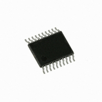
C8051F531-IT Silicon Laboratories Inc, C8051F531-IT Datasheet - Page 54

C8051F531-IT
Manufacturer Part Number
C8051F531-IT
Description
IC 8051 MCU 8K FLASH 20TSSOP
Manufacturer
Silicon Laboratories Inc
Series
C8051F53xr
Specifications of C8051F531-IT
Core Processor
8051
Core Size
8-Bit
Speed
25MHz
Connectivity
SPI, UART/USART
Peripherals
Brown-out Detect/Reset, POR, PWM, Temp Sensor, WDT
Number Of I /o
16
Program Memory Size
8KB (8K x 8)
Program Memory Type
FLASH
Ram Size
256 x 8
Voltage - Supply (vcc/vdd)
2 V ~ 5.25 V
Data Converters
A/D 16x12b
Oscillator Type
Internal
Operating Temperature
-40°C ~ 125°C
Package / Case
20-TSSOP
Data Bus Width
8 bit
Data Ram Size
256 B
Interface Type
SPI, UART
Maximum Clock Frequency
25 MHz
Number Of Programmable I/os
16
Number Of Timers
3
Operating Supply Voltage
2.7 V to 5.25 V
Maximum Operating Temperature
+ 125 C
Mounting Style
SMD/SMT
Minimum Operating Temperature
- 40 C
On-chip Adc
12 bit, 16 Channel
Lead Free Status / RoHS Status
Lead free / RoHS Compliant
Eeprom Size
-
Lead Free Status / Rohs Status
Details
Other names
336-1393
Available stocks
Company
Part Number
Manufacturer
Quantity
Price
Company:
Part Number:
C8051F531-IT
Manufacturer:
SILICON
Quantity:
205
C8051F52x/F52xA/F53x/F53xA
4.3. ADC0 Operation
In a typical system, ADC0 is configured using the following steps:
1. If a gain adjustment is required, refer to Section “4.4. Selectable Gain” on page 60.
2. Choose the start of conversion source.
3. Choose Normal Mode or Burst Mode operation.
4. If Burst Mode, choose the ADC0 Idle Power State and set the Power-Up Time.
5. Choose the tracking mode. Note that Pre-Tracking Mode can only be used with Normal Mode.
6. Calculate required settling time and set the post convert-start tracking time using the AD0TK bits.
7. Choose the repeat count.
8. Choose the output word justification (Right-Justified or Left-Justified).
9. Enable or disable the End of Conversion and Window Comparator Interrupts.
4.3.1. Starting a Conversion
A conversion can be initiated in one of four ways, depending on the programmed states of the ADC0 Start
of Conversion Mode bits (AD0CM1–0) in register ADC0CN. Conversions may be initiated by one of the fol-
lowing:
Writing a 1 to AD0BUSY provides software control of ADC0 whereby conversions are performed "on-
demand.” During conversion, the AD0BUSY bit is set to logic 1 and reset to logic 0 when the conversion is
complete. The falling edge of AD0BUSY triggers an interrupt (when enabled) and sets the ADC0 interrupt
flag (AD0INT). Note: When polling for ADC conversion completions, the ADC0 interrupt flag (AD0INT)
should be used. Converted data is available in the ADC0 data registers, ADC0H:ADC0L, when bit AD0INT
is logic 1. Note that when Timer 2 overflows are used as the conversion source, Low Byte overflows are
used if Timer2 is in 8-bit mode; High byte overflows are used if Timer 2 is in 16-bit mode. See Section
“18. Timers” on page 181 for timer configuration.
Important Note: The CNVSTR input pin also functions as Port pin P0.5 on C8051F52x/52xA devices and
P1.2 on C8051F53x/53xA devices. When the CNVSTR input is used as the ADC0 conversion source, Port
pin P0.5 or P1.2 should be skipped by the Digital Crossbar. To configure the Crossbar to skip P0.5 or P1.2,
set to 1 to the appropriate bit in the PnSKIP register. See Section “13. Port Input/Output” on page 119 for
details on Port I/O configuration.
4.3.2. Tracking Modes
Each ADC0 conversion must be preceded by a minimum tracking time for the converted result to be accu-
rate, as shown in Table 2.3 on page 29. ADC0 has three tracking modes: Pre-Tracking, Post-Tracking, and
Dual-Tracking. Pre-Tracking Mode provides the minimum delay between the convert start signal and end
of conversion by tracking continuously before the convert start signal. This mode requires software man-
agement in order to meet minimum tracking requirements. In Post-Tracking Mode, a programmable track-
ing time starts after the convert start signal and is managed by hardware. Dual-Tracking Mode maximizes
tracking time by tracking before and after the convert start signal. Figure 4.3 shows examples of the three
tracking modes.
Pre-Tracking Mode is selected when AD0TM is set to 10b. Conversions are started immediately following
the convert start signal. ADC0 is tracking continuously when not performing a conversion. Software must
allow at least the minimum tracking time between each end of conversion and the next convert start signal.
The minimum tracking time must also be met prior to the first convert start signal after ADC0 is enabled.
54
Writing a 1 to the AD0BUSY bit of register ADC0CN
A rising edge on the CNVSTR input signal (pin P0.6)
A Timer 1 overflow (i.e., timed continuous conversions)
A Timer 2 overflow (i.e., timed continuous conversions)
Rev. 1.3


