M30833FJGP#D3 Renesas Electronics America, M30833FJGP#D3 Datasheet - Page 14
M30833FJGP#D3
Manufacturer Part Number
M30833FJGP#D3
Description
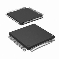
IC M32C MCU FLASH 512K 100LQFP
Manufacturer
Renesas Electronics America
Series
M16C™ M32C/80r
Datasheet
1.M30833FJGPU3.pdf
(96 pages)
Specifications of M30833FJGP#D3
Core Processor
M32C/80
Core Size
16/32-Bit
Speed
32MHz
Connectivity
CAN, I²C, IEBus, SIO, UART/USART
Peripherals
DMA, WDT
Number Of I /o
85
Program Memory Size
512KB (512K x 8)
Program Memory Type
FLASH
Ram Size
31K x 8
Voltage - Supply (vcc/vdd)
3 V ~ 5.5 V
Data Converters
A/D 26x10b; D/A 2x8b
Oscillator Type
Internal
Operating Temperature
-40°C ~ 85°C
Package / Case
100-LQFP
Lead Free Status / RoHS Status
Contains lead / RoHS non-compliant
Eeprom Size
-
Available stocks
Company
Part Number
Manufacturer
Quantity
Price

Part Number:
M30833FJGP#D3M30833FJGP#U3
Manufacturer:
Renesas Electronics America
Quantity:
10 000


R
R
M
e
E
3
. v
J
NOTES:
2
0
10
12
13
14
15
16
17
18
19
20
21
22
23
24
25
26
27
28
29
30
31
32
33
34
35
36
37
38
39
40
41
42
43
44
45
46
47
48
49
50
11
Table 1.5 Pin Characteristics for 100-Pin Package
FP GP
Package
C
1
1
2
3
4
5
6
7
8
9
3
Pin No
1. Bus control pins in M32C/83T cannot be used.
4 .
B
8 /
0
1
100
3
0
99
10
12
13
14
15
16
17
18
19
20
21
22
23
24
25
26
27
28
29
30
31
32
33
34
35
36
37
38
39
40
41
42
43
44
45
46
47
48
11
1
2
3
4
5
6
7
8
9
1
J
G
3
a
o r
0 -
n
BYTE
CNV
X
X
RESET
X
V
X
V
Control
CIN
3 .
COUT
OUT
SS
IN
CC
1
u
Pin
, 1
4
p
/V
SS
1
CONT
(
2
M
0
0
3
6
2
P9
P9
P9
P9
P9
P9
P9
P8
P8
P8
P8
P8
P8
P8
P8
P7
P7
P7
P7
P7
P7
P7
P7
P6
P6
P6
P6
P6
P6
P6
P6
P5
P5
P5
P5
P5
P5
P5
P5
P4
P4
P4
P4
Port
C
6
5
4
3
2
1
0
7
6
5
4
3
2
1
0
7
6
5
4
3
2
1
0
7
6
5
4
3
2
1
0
7
6
5
4
3
2
1
0
7
6
5
4
8 /
Page 12
, 3
Interrupt
NMI
INT2
INT1
INT0
M
Pin
3
2
C
f o
8 /
TB4
TB3
TB2
TB1
TB0
TA4
TA4
TA3
TA3
TA2
TA2
TA1
TA1
TB5
TA0
Timer Pin
9
3
1
IN
OUT
IN
OUT
IN
OUT
IN
OUT
OUT
) T
IN
IN
IN
IN
IN
IN
/U
/W
/V
/TA0
/U
/W
/V
IN
TxD4/SDA4/SRxD4
CLK4
CTS4/RTS4/SS4
CTS3/RTS3/SS3
TxD3/SDA3/SRxD3
RxD3/SCL3/STxD3
CLK3
CAN
CAN
CAN
CAN
CTS2/RTS2/SS2
CLK2
RxD2/SCL2/STxD2
TxD2/SDA2/SRxD2
TxD1/SDA1/SRxD1
RxD1/SCL1/STxD1
CLK1
CTS1/RTS1/SS1
TxD0/SDA0/SRxD0
RxD0/SCL0/STxD0
CLK0
CTS0/RTS0/SS0
UART/CAN Pin
IN
OUT
IN
OUT
OUTC2
IE
OUTC3
OUTC3
INPC0
INPC0
INPC0
INPC1
INPC1
OUTC1
OUTC2
OUTC2
OUTC2
IN
/ISRxD2
0
2
1
2
1
/OUTC0
0
2
0
/ISRxD0/BE0
/OUTC0
/OUTC1
/OUTC1
0
2
0
1
Intelligent I/O Pin
/IE
/ISRxD3
/ISTxD3
/ISTxD1/BE1
/ISRxD2/IE
/ISTxD2/IE
/ISCLK2
OUT
/ISTxD2
0
1
2
1
/ISTxD0/BE0
/ISCLK0
/ISRxD1/BE1
/ISCLK1
OUT
IN
IN
OUT
OUT
IN
ANEX1
ANEX0
DA1
DA0
Analog
Pin
Bus Control Pin
RDY
ALE/RAS
HOLD
HLDA/ALE
CLK
RD/DW
WRH/BHE/CASH
WRL/WR/CASL
CS0/A
CS1/A
CS2/A
CS3/A
OUT
23
22
21
20
/BCLK/ALE
(MA
12
)
(1)
Related parts for M30833FJGP#D3
Image
Part Number
Description
Manufacturer
Datasheet
Request
R

Part Number:
Description:
KIT STARTER FOR M16C/29
Manufacturer:
Renesas Electronics America
Datasheet:

Part Number:
Description:
KIT STARTER FOR R8C/2D
Manufacturer:
Renesas Electronics America
Datasheet:

Part Number:
Description:
R0K33062P STARTER KIT
Manufacturer:
Renesas Electronics America
Datasheet:

Part Number:
Description:
KIT STARTER FOR R8C/23 E8A
Manufacturer:
Renesas Electronics America
Datasheet:

Part Number:
Description:
KIT STARTER FOR R8C/25
Manufacturer:
Renesas Electronics America
Datasheet:

Part Number:
Description:
KIT STARTER H8S2456 SHARPE DSPLY
Manufacturer:
Renesas Electronics America
Datasheet:

Part Number:
Description:
KIT STARTER FOR R8C38C
Manufacturer:
Renesas Electronics America
Datasheet:

Part Number:
Description:
KIT STARTER FOR R8C35C
Manufacturer:
Renesas Electronics America
Datasheet:

Part Number:
Description:
KIT STARTER FOR R8CL3AC+LCD APPS
Manufacturer:
Renesas Electronics America
Datasheet:
Part Number:
Description:
KIT STARTER FOR RX610
Manufacturer:
Renesas Electronics America
Datasheet:

Part Number:
Description:
KIT STARTER FOR R32C/118
Manufacturer:
Renesas Electronics America
Datasheet:

Part Number:
Description:
KIT DEV RSK-R8C/26-29
Manufacturer:
Renesas Electronics America
Datasheet:

Part Number:
Description:
KIT STARTER FOR SH7124
Manufacturer:
Renesas Electronics America
Datasheet:

Part Number:
Description:
KIT STARTER FOR H8SX/1622
Manufacturer:
Renesas Electronics America
Datasheet:

Part Number:
Description:
KIT DEV FOR SH7203
Manufacturer:
Renesas Electronics America
Datasheet: