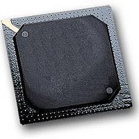
MPC564CZP40 Freescale Semiconductor, MPC564CZP40 Datasheet - Page 6

MPC564CZP40
Manufacturer Part Number
MPC564CZP40
Description
IC MPU 32BIT W/CODE COMP 388PBGA
Manufacturer
Freescale Semiconductor
Series
MPC5xxr
Specifications of MPC564CZP40
Core Processor
PowerPC
Core Size
32-Bit
Speed
40MHz
Connectivity
CAN, EBI/EMI, SCI, SPI, UART/USART
Peripherals
POR, PWM, WDT
Number Of I /o
56
Program Memory Size
512KB (512K x 8)
Program Memory Type
FLASH
Ram Size
32K x 8
Voltage - Supply (vcc/vdd)
2.5 V ~ 2.7 V
Data Converters
A/D 32x10b
Oscillator Type
External
Operating Temperature
-40°C ~ 85°C
Package / Case
388-BGA
Processor Series
MPC5xx
Core
PowerPC
Data Bus Width
32 bit
Data Ram Size
32 KB
Interface Type
CAN, JTAG, QSPI, SCI, SPI, UART
Maximum Clock Frequency
40 MHz
Number Of Programmable I/os
56
Number Of Timers
2
Operating Supply Voltage
0 V to 5 V
Maximum Operating Temperature
+ 85 C
Mounting Style
SMD/SMT
Minimum Operating Temperature
- 40 C
On-chip Adc
2 (10 bit, 32 Channel)
For Use With
MPC564EVB - KIT EVAL FOR MPC561/562/563/564
Lead Free Status / RoHS Status
Contains lead / RoHS non-compliant
Eeprom Size
-
Lead Free Status / Rohs Status
No
Available stocks
Company
Part Number
Manufacturer
Quantity
Price
Company:
Part Number:
MPC564CZP40
Manufacturer:
Freescale Semiconductor
Quantity:
10 000
Key Features
1.2.2
1.2.3
1.2.3.1
1.2.3.2
1.2.3.3
6
•
•
•
•
•
•
•
•
•
•
•
•
•
•
•
•
•
•
•
•
•
•
•
•
•
•
•
•
•
Compliant with Class 3 of the IEEE-ISTO 5001-1999
Program trace via branch trace messaging (BTM)
Data trace via data write messaging (DWM) and data read messaging (DRM)
Ownership trace via ownership trace messaging (OTM)
Run-time access to on-chip memory map and special purpose registers (SPRs) via the READI
read/write access protocol
Watchpoint messaging via the auxiliary port
9 or 16 full-duplex auxiliary pin interface for medium and high visibility throughput
All features configurable and controllable via the auxiliary port
Security features for production environment
Supports the RCPU debug mode via the auxiliary port
READI module can be reset independent of system reset
True 5 V I/O
Two time processing units (TPU3) with 16 channels each
Each TPU3 is a micro-coded timer subsystem
8 Kbytes of dual port TPU RAM (DPTRAM) shared by two TPU3 modules for TPU micro-code
Six modulus counter sub-modules (MCSM)
10 double-action sub-modules (DASM)
12 dedicated PWM sub-modules (PWMSM)
One MIOS14 16-bit parallel port I/O sub-modules (MPIOSM)
Two queued analog-to-digital converter modules (QADC64E_A, QADC64_B) providing a total of
32 analog channels
16 analog input channels on each QADC64E_A module using internal multiplexing
Directly supports up to four external multiplexers
Up to 41 total input channels on the two QADC64E modules with external multiplexing
Software configurable to operate in enhanced or legacy (MPC555 compatible) mode
Unused analog channels can be used as digital input/output pins
GPIO on all channels in enhanced mode
10-bit A/D converter with internal sample/hold
Typical conversion time of less than 5 µs (>200 K samples/second)
Two conversion command queues of variable length
Nexus Debug Port (Class 3)
Integrated I/O System
Two Time Processor Units (TPU3)
22-Channel Modular I/O System (MIOS14)
Two Enhanced Queued Analog-to-Digital Converter Modules
(QADC64E)
Freescale Semiconductor, Inc.
For More Information On This Product,
MPC561/MPC563 Product Brief
Go to: www.freescale.com
MOTOROLA


