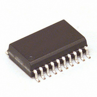
MC68HC908JK3CDW Freescale Semiconductor, MC68HC908JK3CDW Datasheet - Page 43

MC68HC908JK3CDW
Manufacturer Part Number
MC68HC908JK3CDW
Description
IC MCU 8MHZ 4K FLASH 20-SOIC
Manufacturer
Freescale Semiconductor
Series
HC08r
Datasheet
1.MC68HC908JK1CDW.pdf
(212 pages)
Specifications of MC68HC908JK3CDW
Core Processor
HC08
Core Size
8-Bit
Speed
8MHz
Peripherals
LED, LVD, POR, PWM
Number Of I /o
15
Program Memory Size
4KB (4K x 8)
Program Memory Type
FLASH
Ram Size
128 x 8
Voltage - Supply (vcc/vdd)
2.7 V ~ 3.3 V
Data Converters
A/D 12x8b
Oscillator Type
External
Operating Temperature
-40°C ~ 85°C
Package / Case
20-SOIC (7.5mm Width)
Lead Free Status / RoHS Status
Contains lead / RoHS non-compliant
Eeprom Size
-
Connectivity
-
- Current page: 43 of 212
- Download datasheet (3Mb)
4.7 FLASH Program Operation
MC68H(R)C908JL3
Freescale Semiconductor
NOTE:
—
Rev. 1.1
Programming of the FLASH memory is done on a row basis. A row
consists of 32 consecutive bytes starting from addresses $XX00,
$XX20, $XX40, $XX60, $XX80, $XXA0, $XXC0 or $XXE0. Use this
step-by-step procedure to program a row of FLASH memory:
(Figure 4-2
In order to avoid program disturbs, the row must be erased before any
byte on that row is programmed.
This program sequence is repeated throughout the memory until all data
is programmed.
10. Wait for time, t
11. Clear the HVEN bit.
12. After time, t
1. Set the PGM bit. This configures the memory for program
2. Write any data to any FLASH location within the address range of
3. Wait for a time, t
4. Set the HVEN bit.
5. Wait for a time, t
6. Write data to the byte being programmed.
7. Wait for time, t
8. Repeat step 6 and 7 until all the bytes within the row are
9. Clear the PGM bit.
operation and enables the latching of address and data for
programming.
the row to be programmed.
programmed.
again.
shows a flowchart of the programming algorithm.)
FLASH Memory (FLASH)
rcv
PROG
nvh
(1µs), the memory can be accessed in read mode
nvs
pgs
(5µs).
(10µs).
(5µs).
(30µs).
FLASH Memory (FLASH)
Technical Data
43
Related parts for MC68HC908JK3CDW
Image
Part Number
Description
Manufacturer
Datasheet
Request
R
Part Number:
Description:
Manufacturer:
Freescale Semiconductor, Inc
Datasheet:
Part Number:
Description:
Manufacturer:
Freescale Semiconductor, Inc
Datasheet:
Part Number:
Description:
Manufacturer:
Freescale Semiconductor, Inc
Datasheet:
Part Number:
Description:
Manufacturer:
Freescale Semiconductor, Inc
Datasheet:
Part Number:
Description:
Manufacturer:
Freescale Semiconductor, Inc
Datasheet:
Part Number:
Description:
Manufacturer:
Freescale Semiconductor, Inc
Datasheet:
Part Number:
Description:
Manufacturer:
Freescale Semiconductor, Inc
Datasheet:
Part Number:
Description:
Manufacturer:
Freescale Semiconductor, Inc
Datasheet:
Part Number:
Description:
Manufacturer:
Freescale Semiconductor, Inc
Datasheet:
Part Number:
Description:
Manufacturer:
Freescale Semiconductor, Inc
Datasheet:
Part Number:
Description:
Manufacturer:
Freescale Semiconductor, Inc
Datasheet:
Part Number:
Description:
Manufacturer:
Freescale Semiconductor, Inc
Datasheet:
Part Number:
Description:
Manufacturer:
Freescale Semiconductor, Inc
Datasheet:
Part Number:
Description:
Manufacturer:
Freescale Semiconductor, Inc
Datasheet:
Part Number:
Description:
Manufacturer:
Freescale Semiconductor, Inc
Datasheet:


