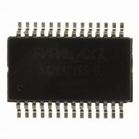
SX28AC/SS-G Parallax Inc, SX28AC/SS-G Datasheet - Page 27

SX28AC/SS-G
Manufacturer Part Number
SX28AC/SS-G
Description
IC RISC MCU 2KX12 EE/FLASH28S
Manufacturer
Parallax Inc
Series
SXr
Datasheet
1.SX20ACSS-G.pdf
(51 pages)
Specifications of SX28AC/SS-G
Core Size
8-Bit
Program Memory Size
3KB (2K x 12)
Oscillator Type
Internal
Core Processor
RISC
Speed
75MHz
Peripherals
Brown-out Detect/Reset, POR, WDT
Number Of I /o
20
Program Memory Type
FLASH
Ram Size
136 x 8
Voltage - Supply (vcc/vdd)
3 V ~ 5.5 V
Operating Temperature
0°C ~ 70°C
Package / Case
28-DIP (0.300", 7.62mm)
Controller Family/series
SX
No. Of I/o's
20
Eeprom Memory Size
2048Byte
Ram Memory Size
136Byte
Cpu Speed
75MHz
Processor Series
Ubicom SXx
Core
RISC
Data Bus Width
8 bit
Data Ram Size
136 B
Maximum Clock Frequency
75 MHz
Number Of Programmable I/os
20
Number Of Timers
1
Operating Supply Voltage
4.5 V to 5.5 V
Maximum Operating Temperature
+ 70 C
Mounting Style
SMD/SMT
Development Tools By Supplier
32300, 45302
Minimum Operating Temperature
0 C
Lead Free Status / RoHS Status
Lead free / RoHS Compliant
Eeprom Size
-
Data Converters
-
Connectivity
-
Lead Free Status / Rohs Status
Details
Available stocks
Company
Part Number
Manufacturer
Quantity
Price
Company:
Part Number:
SX28AC/SS-G
Manufacturer:
UBKOM
Quantity:
5 510
Part Number:
SX28AC/SS-G
Manufacturer:
SCENIX
Quantity:
20 000
Parallax SX20AC/SX28AC
11.0 COMPARATOR
The device contains an on-chip differential comparator.
Ports RB0-RB2 support the comparator. Ports RB1 and
RB2 are the comparator negative and positive inputs,
respectively, while Port RB0 serves as the comparator
output pin. To use these pins in conjunction with the
comparator, the user program must configure Ports RB1
and RB2 as inputs and Port RB0 as an output. The
CMP_B register is used to enable the comparator, to read
the output of the comparator internally, and to enable the
output of the comparator to the comparator output pin.
The comparator enable bits are set to “1” upon reset, thus
disabling the comparator. To avoid drawing additional
current during the power down mode, the comparator
should be disabled before entering the power down mode.
Here is an example of how to setup the comparator and
read the CMP_B register.
mov
mov
mov
mov
mov
mov
and
snb
jmp
© Parallax Inc.
M,#$08 ;set MODE register to access
W,#$00 ;clear W
!RB,W
M,#$08 ;set MODE register to access
W,#$00 ;clear W
!RB,W
W,#$01 ;set/clear Z bit based on
$03.2
rb2_hi ;jump only if RB2>RB1
;CMP_B
;enable comparator and its
;output
;delay after enabling
;comparator for response
;CMP_B
;enable comparator and its
;output and also read CMP_B
;(exchange W and CMB_B)
;comparator result
;test Z bit in STATUS reg
;(0 => RB2<RB1)
Page 27 of 51
The final “mov” instruction in this example performs an
exchange of data between the working register (W) and
the CMP_B register. This exchange occurs only with Port
B accesses. Otherwise, the “mov” instruction does not
perform an exchange, but only moves data from the
source to the destination.
Figure 11-1 shows the comparator block diagram.
CMP_B - Comparator Enable/Status Register
CMP _
CMP _
CMP _
CMP
Bit 7
EN
OE
RES
_
EN
CMP
Comparator result: 1 for RB2>RB1 or 0
for RB2<RB1. Comparator must be
enabled (CMP_EN = 0) to read the
result. The result can be read whether or
not the CMP_OE bit is cleared.
When cleared to 0, it enables the
comparator output to the RB0 pin.
When cleared to 0, it enables the
comparator.
Bit 6
_
OE
Figure 11-1:
Comparator
Block Diagram
Reserved
Bits 5-1
Rev 1.6 11/20/2006
www.parallax.com
CMP_RES
Bit 0


