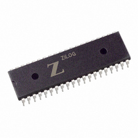
ZGP323LAP4008G Zilog, ZGP323LAP4008G Datasheet - Page 14

ZGP323LAP4008G
Manufacturer Part Number
ZGP323LAP4008G
Description
IC Z8 GP MCU 8K OTP 40DIP
Manufacturer
Zilog
Series
Z8® GP™r
Specifications of ZGP323LAP4008G
Core Processor
Z8
Core Size
8-Bit
Speed
8MHz
Peripherals
HLVD, POR, WDT
Number Of I /o
32
Program Memory Size
8KB (8K x 8)
Program Memory Type
OTP
Ram Size
237 x 8
Voltage - Supply (vcc/vdd)
2 V ~ 3.6 V
Oscillator Type
Internal
Operating Temperature
-40°C ~ 125°C
Package / Case
40-DIP (0.620", 15.75mm)
Lead Free Status / RoHS Status
Lead free / RoHS Compliant
Eeprom Size
-
Data Converters
-
Connectivity
-
Other names
269-4425
ZGP323LAP4008G
ZGP323LAP4008G
Pin Functions
PS023709-0208
Caution:
XTAL1 Crystal 1 (Time-Based Input)
XTAL2 Crystal 2 (Time-Based Output)
Input/Output Ports
This pin connects a parallel-resonant crystal or ceramic resonator to the on-chip oscillator
input. Additionally, an optional external single-phase clock can be coded to the on-chip
oscillator input.
This pin connects a parallel-resonant crystal or ceramic resonant to the on-chip oscillator
output.
Input/Output ports are described in the following sections.
The CMOS input buffer for each port 0, 1, or 2 pin is always connected to the pin, even
when the pin is configured as an output. If the pin is configured as an open-drain output
and no signal is applied, a High output state can cause the CMOS input buffer to float.
This might lead to excessive leakage current of more than 100 µA. To prevent this leak-
age, connect the pin to an external signal with a defined logic level or ensure its output
state is Low, especially during STOP mode.
Internal pull-ups are disabled on any given pin or group of port pins when programmed
into output mode.
Port 0, 1 and 2 have both input and output capability. The input logic is always present
no matter whether the port is configured as input or output. When doing a READ in-
struction, it will read the actual value at the input logic not from the output buffer.
In addition, the instruction of "OR", "AND", "XOR" are read-modify-write instructions.
It will first read the port and then modify the value and load back to the port.
Precaution must be taken if the port is configured as open-drain output or driving some
circuit that may make the voltage different from the desired output logic. For example,
pins P00-P07 are not connecting to anything else. If it is configured as open-drain
output with outputting logic ONE, it is a floating port and will read back as ZERO. The
following instruction will set P00-P07 all LOW.
AND P0,#%F0
Product Specification
Pin Description
ZGP323L
10


