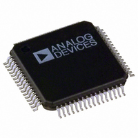
ADUC7024BST62-REEL Analog Devices Inc, ADUC7024BST62-REEL Datasheet - Page 18

ADUC7024BST62-REEL
Manufacturer Part Number
ADUC7024BST62-REEL
Description
IC MCU FLASH 62K W/ANLG 64-LQFP
Manufacturer
Analog Devices Inc
Series
MicroConverter® ADuC7xxxr
Datasheet
1.USB-I2CLIN-CONV-Z.pdf
(96 pages)
Specifications of ADUC7024BST62-REEL
Rohs Status
RoHS non-compliant
Design Resources
Sensing Low-g Acceleration Using ADXL345 Digital Accelerometer Connected to ADuC7024 (CN0133)
Core Processor
ARM7
Core Size
16/32-Bit
Speed
44MHz
Connectivity
EBI/EMI, I²C, SPI, UART/USART
Peripherals
PLA, PWM, PSM, Temp Sensor, WDT
Number Of I /o
30
Program Memory Size
62KB (62K x 8)
Program Memory Type
FLASH
Ram Size
8K x 8
Voltage - Supply (vcc/vdd)
2.7 V ~ 3.6 V
Data Converters
A/D 10x12b; D/A 2x12b
Oscillator Type
Internal
Operating Temperature
-40°C ~ 125°C
Package / Case
64-LQFP
Eeprom Size
-
Other names
ADUC7024BST62REEL
ADuC7019/20/21/22/24/25/26/27/28/29
Table 11. Pin Function Descriptions (ADuC7019/ADuC7020/ADuC7021/ADuC7022)
7019/7020
38
39
40
1
2
‒
‒
‒
‒
‒
3
4
5
6
7
8
9
Pin No.
7021
37
38
39
40
1
2
3
4
‒
‒
5
6
7
‒
‒
8
9
7022
36
37
38
39
40
1
2
3
4
5
6
‒
‒
‒
‒
7
8
Mnemonic
ADC0
ADC1
ADC2/CMP0
ADC3/CMP1
ADC4
ADC5
ADC6
ADC7
ADC8
ADC9
GND
DAC0/ADC12
DAC1/ADC13
DAC2/ADC14
DAC3/ADC15
TMS
TDI
BM/P0.0/CMP
NOTES
1. THE EXPOSED PADDLE MUST BE LEFT UNCONNECTED.
P0.6/T1/MRST/PLAO[3]
REF
OUT
GND
/PLAI[7]
Figure 12. 40-Lead LFCSP_VQ Pin Configuration (ADuC7022)
ADC5
ADC6
ADC7
ADC8
ADC9
TMS
REF
TDI
10
1
2
3
4
5
6
7
8
9
PIN 1
INDICATOR
Rev. C | Page 18 of 96
ADuC7022
(Not to Scale)
TOP VIEW
Single-Ended or Differential Analog Input 0.
Single-Ended or Differential Analog Input 1.
Single-Ended or Differential Analog Input 2/Comparator Positive Input.
Single-Ended or Differential Analog Input 3 (Buffered Input on ADuC7019)/
Comparator Negative Input.
Single-Ended or Differential Analog Input 4.
Single-Ended or Differential Analog Input 5.
Single-Ended or Differential Analog Input 6.
Single-Ended or Differential Analog Input 7.
Single-Ended or Differential Analog Input 8.
Single-Ended or Differential Analog Input 9.
Ground Voltage Reference for the ADC. For optimal performance, the
analog power supply should be separated from IOGND and DGND.
DAC0 Voltage Output/Single-Ended or Differential Analog Input 12.
DAC1 Voltage Output/Single-Ended or Differential Analog Input 13.
DAC2 Voltage Output/Single-Ended or Differential Analog Input 14.
DAC3 Voltage Output on ADuC7020. On the ADuC7019, a 10 nF capacitor
must be connected between this pin and AGND/Single-Ended or
Differential Analog Input 15 (see Figure 43).
Test Mode Select, JTAG Test Port Input. Debug and download access.
This pin has an internal pull-up resistor to IOV
pull-up resistor (~100K) is also required to ensure that the part does not
enter an erroneous state.
Test Data In, JTAG Test Port Input. Debug and download access.
Description
30
29
28
27
26
25
24
23
22
21
P1.2/SPM2/PLAI[2]
P1.3/SPM3/PLAI[3]
P1.4/SPM4/PLAI[4]/IRQ2
P1.5/SPM5/PLAI[5]/IRQ3
P1.6/SPM6/PLAI[6]
P1.7/SPM7/PLAO[0]
XCLKI
XCLKO
P0.7/ECLK/XCLK/SPM8/PLAO[4]
P2.0/SPM9/PLAO[5]/CONV
START
DD
. In some cases, an external


