TS87C51RC2-VIE Atmel, TS87C51RC2-VIE Datasheet
TS87C51RC2-VIE
Specifications of TS87C51RC2-VIE
Available stocks


Related parts for TS87C51RC2-VIE


TS87C51RC2-VIE Summary of contents
Page 1
... High Performance 8-bit Microcontrollers 1. Description Atmel Wireless & Microcontrollers TS80C51Rx2 is high performance CMOS ROM, OTP, EPROM and ROMless versions of the 80C51 CMOS single chip 8-bit microcontroller. The TS80C51Rx2 retains all features of the 80C51 with extended ROM/EPROM capacity (16/32/64 Kbytes), 256 bytes of internal RAM, a 7-source , 4-level interrupt system, an on-chip oscilator and three timer/counters ...
Page 2
... TS80C51RA2/RD2 TS83C51RB2/RC2/RD2 TS87C51RB2/RC2/RD2 PDIL40 PLCC44 ROM (bytes) VQFP44 1.4 TS80C51RA2 0 TS80C51RD2 0 TS83C51RB2 16k TS83C51RC2 32k TS83C51RD2 64k TS87C51RB2 0 TS87C51RC2 0 TS87C51RD2 0 PLCC68 ROM (bytes) VQFP64 1.4 TS80C51RD2 0 TS83C51RD2 64k TS87C51RD2 0 3. Block Diagram (3) XTAL1 XTAL2 ALE/ PROG PSEN CPU EA/V PP (3) RD (3) ...
Page 3
SFR Mapping The Special Function Registers (SFRs) of the TS80C51Rx2 fall into the following categories: C51 core registers: ACC, B, DPH, DPL, PSW, SP, AUXR1 I/O port registers: P0, P1, P2, P3, P4, P5 Timer registers: T2CON, T2MOD, TCON, ...
Page 4
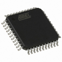
TS80C51RA2/RD2 TS83C51RB2/RC2/RD2 TS87C51RB2/RC2/RD2 5. Pin Configuration P1 VCC 39 P0 P1.1 / T2EX P1.2 3 P1 P1.4 5 P0.4 / ...
Page 5
P5.5 P0.3/AD3 P0.2/AD2 P5.6 P0.1/AD1 P0.0/AD0 P5.7 VCC NIC P1.0/T2 P4.0 P1.1/T2EX P1.2 P1.3 P4.1 P1.4 P4.2 P0.3/AD3 P0.2/AD2 P0.1/AD1 P0.0/AD0 VCC P1.0/T2 P1.1/T2EX NIC: No InternalConnection Rev March, 2001 ...
Page 6
TS80C51RA2/RD2 TS83C51RB2/RC2/RD2 TS87C51RB2/RC2/RD2 Pin Number Mnemonic DIL LCC VQFP 1 Vss1 P0.0-P0.7 39-32 43-36 37-30 P1.0-P1.7 1-8 2-9 40-44 1 ...
Page 7
Reset Rev March, 2001 TS83C51RB2/RC2/RD2 TS87C51RB2/RC2/RD2 I Reset: A high on this pin for two machine cycles while the oscillator is running, resets the device. An internal diffused resistor to V using only an ...
Page 8
TS80C51RA2/RD2 TS83C51RB2/RC2/RD2 TS87C51RB2/RC2/RD2 Pin Number Mnemonic ALE/PROG PSEN EA XTAL1 XTAL2 Type Name And Function O (I) Address Latch Enable/Program Pulse: Output pulse ...
Page 9
Pin Description for 64/68 pin Packages Port 4 and Port 5 are 8-bit bidirectional I/O ports with internal pull-ups. Pins that have 1 written to them are pulled high by the internal pull ups and can be used as ...
Page 10
TS80C51RA2/RD2 TS83C51RB2/RC2/RD2 TS87C51RB2/RC2/RD2 P3.2 P3.3 P3.4 P3.5 P3.6 P3.7 RESET ALE/PROG PSEN EA/VPP XTAL1 XTAL2 P4.0 P4.1 P4.2 P4.3 P4.4 P4.5 P4.6 P4.7 P5.0 P5.1 P5.2 P5.3 P5.4 P5.5 P5.6 P5.7 10 SQUARE VQFP64 PLCC68 1 ...
Page 11
TS80C51Rx2 Enhanced Features In comparison to the original 80C52, the TS80C51Rx2 implements some new features, which are The X2 option. The Dual Data Pointer. The extended RAM. The Programmable Counter Array (PCA). The Watchdog. The 4 level interrupt priority ...
Page 12
TS80C51RA2/RD2 TS83C51RB2/RC2/RD2 TS87C51RB2/RC2/RD2 XTAL1 XTAL1:2 X2 bit CPU clock STD Mode The X2 bit in the CKCON register (See Table 3.) allows to switch from 12 clock cycles per instruction to 6 clock cycles and vice versa. At reset, the ...
Page 13
... Clear to select 12 clock periods per machine cycle (STD mode Set to select 6 clock periods per machine cycle (X2 mode, F Reset Value = XXXX XXX0b Not bit addressable For further details on the X2 feature, please refer to ANM072 available on the web (http://www.atmel-wm.com) Rev March, 2001 Table 3. CKCON Register ...
Page 14
TS80C51RA2/RD2 TS83C51RB2/RC2/RD2 TS87C51RB2/RC2/RD2 6.2. Dual Data Pointer Register Ddptr The additional data pointer can be used to speed up code execution and reduce code size in a number of ways. The dual DPTR structure is a way by which the ...
Page 15
ASSEMBLY LANGUAGE ; Block move using dual data pointers ; Destroys DPTR0, DPTR1, A and PSW ; note: DPS exits opposite of entry state ; unless an extra INC AUXR1 is added ; 00A2 AUXR1 EQU 0A2H ; 0000 909000 ...
Page 16
TS80C51RA2/RD2 TS83C51RB2/RC2/RD2 TS87C51RB2/RC2/RD2 6.3. Expanded RAM (XRAM) The TS80C51Rx2 provide additional Bytes of ramdom access memory (RAM) space for increased data parameter handling and high level language usage. RA2, RB2 and RC2 devices have 256 bytes of expanded RAM, from ...
Page 17
FF(RA, RB, RC)/2FF (RD) XRAM 256 bytes 00 Figure 4. Internal and External Data Memory Address AUXR Address 08EH Reset value Symbol - AO EXTRAM a. User software should not write 1s to reserved bits. These bits may be used ...
Page 18
... Auto-Reload Mode The auto-reload mode configures timer 16-bit timer or event counter with automatic reload. If DCEN bit in T2MOD is cleared, timer 2 behaves as in 80C52 (refer to the Atmel Wireless & Microcontrollers 8-bit Microcontroller Hardware description). If DCEN bit is set, timer 2 acts as an Up/down timer/counter as shown in Figure 5 ...
Page 19
XTAL1 F XTAL Figure 5. Auto-Reload Mode Up/Down Counter (DCEN = 1) 6.4.2. Programmable Clock-Output In the clock-out mode, timer 2 operates as a 50%-duty-cycle, programmable clock generator (See Figure 6) . The input clock increments TL2 at frequency F ...
Page 20
TS80C51RA2/RD2 TS83C51RB2/RC2/RD2 TS87C51RB2/RC2/RD2 It is possible to use timer baud rate generator and a clock generator simultaneously. For this configuration, the baud rates and clock frequencies are not independent since both functions use the values in the ...
Page 21
T2CON - Timer 2 Control Register (C8h TF2 EXF2 RCLK Bit Bit Number Mnemonic Timer 2 overflow Flag 7 TF2 Must be cleared by software. Set by hardware on timer 2 overflow, if RCLK = 0 and TCLK ...
Page 22
TS80C51RA2/RD2 TS83C51RB2/RC2/RD2 TS87C51RB2/RC2/RD2 T2MOD - Timer 2 Mode Control Register (C9h Bit Bit Number Mnemonic Reserved 7 - The value read from this bit is indeterminate. Do not set this bit. Reserved 6 - The value ...
Page 23
Programmable Counter Array PCA The PCA provides more timing capabilities with less CPU intervention than the standard timer/counters. Its advantages include reduced software overhead and improved accuracy. The PCA consists of a dedicated timer/counter which serves as the time ...
Page 24
TS80C51RA2/RD2 TS83C51RB2/RC2/RD2 TS87C51RB2/RC2/RD2 Fosc /12 Fosc / 4 T0 OVF P1.2 CIDL Idle CF Table 8. CMOD: PCA Counter Mode Register CMOD Address 0D9H Reset value Symbol CIDL WDTE - CPS1 CPS0 ECF a. User software should not write 1s ...
Page 25
The ECF bit which when set causes an interrupt and the PCA overflow flag CF (in the CCON SFR set when the PCA timer overflows. Rev March, 2001 TS80C51RA2/RD2 TS83C51RB2/RC2/RD2 TS87C51RB2/RC2/RD2 25 ...
Page 26
TS80C51RA2/RD2 TS83C51RB2/RC2/RD2 TS87C51RB2/RC2/RD2 The CCON SFR contains the run control bit for the PCA and the flags for the PCA timer (CF) and each module (Refer to Table 9). Bit CR (CCON.6) must be set by software to run the ...
Page 27
PCA Timer/Counter Module 0 Module 1 Module 2 Module 3 Module 4 CMOD.0 ECF PCA Modules: each one of the five compare/capture modules has six possible functions. It can perform: • 16-bit Capture, positive-edge triggered, • 16-bit Capture, negative-edge triggered, ...
Page 28
TS80C51RA2/RD2 TS83C51RB2/RC2/RD2 TS87C51RB2/RC2/RD2 Table 10. CCAPMn: PCA Modules Compare/Capture Control Registers CCAPM0=0DAH CCAPM1=0DBH CCAPMn Address CCAPM2=0DCH CCAPM3=0DDH CCAPM4=0DEH Reset value Symbol - ECOMn CAPPn CAPNn MATn TOGn PWMn ECCFn a. User software should not write ...
Page 29
Table 12. CCAPnH: PCA Modules Capture/Compare Registers High CCAP0H=0FAH CCAP1H=0FBH CCAPnH Address CCAP2H=0FCH CCAP3H=0FDH CCAP4H=0FEH Reset value Table 13. CCAPnL: PCA Modules Capture/Compare Registers Low CCAP0L=0EAH CCAP1L=0EBH CCAPnL Address CCAP2L=0ECH ...
Page 30
TS80C51RA2/RD2 TS83C51RB2/RC2/RD2 TS87C51RB2/RC2/RD2 6.5.1. PCA Capture Mode To use one of the PCA modules in the capture mode either one or both of the CCAPM bits CAPN and CAPP for that module must be set. The external CEX input for ...
Page 31
Software Timer / Compare Mode The PCA modules can be used as software timers by setting both the ECOM and MAT bits in the modules CCAPMn register. The PCA timer will be compared to the module's capture registers ...
Page 32
TS80C51RA2/RD2 TS83C51RB2/RC2/RD2 TS87C51RB2/RC2/RD2 6.5.3. High Speed Output Mode In this mode the CEX output (on port 1) associated with the PCA module will toggle each time a match occurs between the PCA counter and the module's capture registers. To activate ...
Page 33
Pulse Width Modulator Mode All of the PCA modules can be used as PWM outputs. Figure 12 shows the PWM function. The frequency of the output depends on the source for the PCA timer. All of the modules will ...
Page 34
TS80C51RA2/RD2 TS83C51RB2/RC2/RD2 TS87C51RB2/RC2/RD2 6.6. TS80C51Rx2 Serial I/O Port The serial I/O port in the TS80C51Rx2 is compatible with the serial I/O port in the 80C52. It provides both synchronous and asynchronous communication modes. It operates as an Universal Asynchronous Receiver ...
Page 35
Software may examine FE bit after each reception to check for data errors. Once set, only software or a reset can clear FE bit. Subsequently received frames with valid stop bits cannot clear FE bit. When FE feature is enabled, ...
Page 36
TS80C51RA2/RD2 TS83C51RB2/RC2/RD2 TS87C51RB2/RC2/RD2 6.6.3. Given Address Each device has an individual address that is specified in SADDR register; the SADEN register is a mask byte that contains don’t-care bits (defined by zeros) to form the device’s given address. The don’t-care ...
Page 37
Reset Addresses On reset, the SADDR and SADEN registers are initialized to 00h, i.e. the given and broadcast addresses are XXXX XXXXb (all don’t-care bits). This ensures that the serial port will reply to any address, and so, that ...
Page 38
TS80C51RA2/RD2 TS83C51RB2/RC2/RD2 TS87C51RB2/RC2/RD2 SCON - Serial Control Register (98h FE/SM0 SM1 SM2 Bit Bit Number Mnemonic Framing Error bit (SMOD0=1) Clear to reset the error state, not cleared by a valid stop bit Set by hardware ...
Page 39
PCON - Power Control Register (87h SMOD1 SMOD0 Bit Bit Number Mnemonic Serial port Mode bit 1 7 SMOD1 Set to select double baud rate in mode Serial port Mode bit 0 6 SMOD0 ...
Page 40
TS80C51RA2/RD2 TS83C51RB2/RC2/RD2 TS87C51RB2/RC2/RD2 6.7. Interrupt System The TS80C51Rx2 has a total of 7 interrupt vectors: two external interrupts (INT0 and INT1), three timer interrupts (timers 0, 1 and 2), the serial port interrupt and the PCA global interrupt. These interrupts ...
Page 41
IPH low-priority interrupt can be interrupted by a high priority interrupt, but not by another low-priority interrupt. A high-priority interrupt can’t be interrupted by any other interrupt source. If two interrupt requests of different priority ...
Page 42
TS80C51RA2/RD2 TS83C51RB2/RC2/RD2 TS87C51RB2/RC2/RD2 IP - Interrupt Priority Register (B8h PPC PT2 Bit Bit Number Mnemonic Reserved 7 - The value read from this bit is indeterminate. Do not set this bit. PCA interrupt priority bit 6 PPC ...
Page 43
IPH - Interrupt Priority High Register (B7h PPCH PT2H Bit Bit Number Mnemonic Reserved 7 - The value read from this bit is indeterminate. Do not set this bit. PCA interrupt priority bit high. PPCH 0 0 ...
Page 44
TS80C51RA2/RD2 TS83C51RB2/RC2/RD2 TS87C51RB2/RC2/RD2 6.8. Idle mode An instruction that sets PCON.0 causes that to be the last instruction executed before going into the Idle mode. In the Idle mode, the internal clock signal is gated off to the CPU, but ...
Page 45
Table 22. The state of ports during idle and power-down mode Program Mode ALE Memory Idle Internal Idle External Power Down Internal Power Down External * Port 0 can force a "zero" level. A "one" will leave port floating. Rev. ...
Page 46
TS80C51RA2/RD2 TS83C51RB2/RC2/RD2 TS87C51RB2/RC2/RD2 6.10. Hardware Watchdog Timer The WDT is intended as a recovery method in situations where the CPU may be subjected to software upset. The WDT consists of a 14-bit counter and the WatchDog Timer ReSeT (WDTRST) SFR. ...
Page 47
WDTPRG Address (0A7h Bit Bit Number Mnemonic Reserved not try to set or clear this bit WDT Time-out select bit 2 1 ...
Page 48
TS80C51RA2/RD2 TS83C51RB2/RC2/RD2 TS87C51RB2/RC2/RD2 TM 6.11. ONCE Mode (ON Chip Emulation) The ONCE mode facilitates testing and debugging of systems using TS80C51Rx2 without removing the circuit from the board. The ONCE mode is invoked by driving certain pins of the TS80C51Rx2; ...
Page 49
Power-Off Flag The power-off flag allows the user to distinguish between a “cold start” reset and a “warm start” reset. A cold start reset is the one induced by V the device and could be generated for example by ...
Page 50
TS80C51RA2/RD2 TS83C51RB2/RC2/RD2 TS87C51RB2/RC2/RD2 6.13. Reduced EMI Mode The ALE signal is used to demultiplex address and data buses on port 0 when used with external program or data memory. Nevertheless, during internal code execution, ALE signal is still generated. In ...
Page 51
TS83C51RB2/RC2/RD2 ROM 7.1. ROM Structure The TS83C51RB2/RC2/RD2 ROM memory is divided in three different arrays: the code array ...
Page 52
TS80C51RA2/RD2 TS83C51RB2/RC2/RD2 TS87C51RB2/RC2/RD2 8. TS87C51RB2/RC2/RD2 EPROM 8.1. EPROM Structure The TS87C51RB2/RC2/RD2 EPROM is divided in two different arrays: the code array ...
Page 53
EPROM Programming 8.3.1. Set-up modes In order to program and verify the EPROM or to read the signature bytes, the TS87C51RB2/RC2/RD2 is placed in specific set-up modes (See Figure 18.). Control and program signals must be held at the ...
Page 54
TS80C51RA2/RD2 TS83C51RB2/RC2/RD2 TS87C51RB2/RC2/RD2 PROGRAM SIGNALS* CONTROL SIGNALS MHz * See Table 31. for proper value on these inputs 8.3.3. Programming Algorithm The Improved Quick Pulse algorithm is based on the Quick Pulse algorithm and decreases the number ...
Page 55
Programming Cycle A0-A12 D0-D7 ALE/PROG 12.75V 5V EA/VPP 0V Control sig- nals Figure 19. Programming and Verification Signal’s Waveform 8.4. EPROM Erasure (Windowed Packages Only) Erasing the EPROM erases the code array, the encryption array and the lock bits returning ...
Page 56
... Manufacturer Code: Atmel Wireless & Microcontrollers 57h Family Code: C51 X2 7Ch Product name: TS83C51RD2 FCh Product name: TS87C51RD2 37h Product name: TS83C51RC2 B7h Product name: TS87C51RC2 3Bh Product name: TS83C51RB2 BBh Product name: TS87C51RB2 FFh Product revision number Comment Rev March, 2001 ...
Page 57
... Since the introduction of the first C51 devices, every manufacturer made operating Icc measurements under reset, which made sense for the designs were the CPU was running under reset. In Atmel Wireless & Microcontrollers new devices, the CPU is no more active during reset, so the power consumption is very low but is not really representative of what will happen in the customer system. That’ ...
Page 58
TS80C51RA2/RD2 TS83C51RB2/RC2/RD2 TS87C51RB2/RC2/RD2 10.3. DC Parameters for Standard Voltage + - + Table 32. DC ...
Page 59
Symbol Parameter I Power Supply Current Maximum values (7) mode: operating I Power Supply Current Maximum values (7) mode: idle 10.4. DC Parameters for Low Voltage + ...
Page 60
TS80C51RA2/RD2 TS83C51RB2/RC2/RD2 TS87C51RB2/RC2/RD2 Symbol Parameter I Power Supply Current Maximum values (7) mode: idle NOTES 1. I under reset is measured with all output pins disconnected; XTAL1 driven with 0.5V; XTAL2 N.C.; ...
Page 61
Reset = Vss after a high pulse during at least 24 clock cycles Reset = Vss after a high pulse during at least 24 clock cycles Reset = Vss after a high pulse during at least 24 clock cycles Figure ...
Page 62
TS80C51RA2/RD2 TS83C51RB2/RC2/RD2 TS87C51RB2/RC2/RD2 10.5. AC Parameters 10.5.1. Explanation of the AC Symbols Each timing symbol has 5 characters. The first character is always a “T” (stands for time). The other characters, depending on their positions, stand for the name of ...
Page 63
External Program Memory Characteristics Symbol T Oscillator clock period T ALE pulse width LHLL T Address Valid to ALE AVLL T Address Hold After ALE LLAX T ALE to Valid Instruction In LLIV T ALE to PSEN LLPL T ...
Page 64
TS80C51RA2/RD2 TS83C51RB2/RC2/RD2 TS87C51RB2/RC2/RD2 Table 38. AC Parameters for a Variable Clock: derating formula Symbol Type Standard Clock T Min LHLL T Min AVLL T Min LLAX T Max 4 T ...
Page 65
External Data Memory Characteristics Symbol T RD Pulse Width RLRH T WR Pulse Width WLWH Valid Data In RLDV T Data Hold After RD RHDX T Data Float After RD RHDZ T ALE to Valid Data ...
Page 66
TS80C51RA2/RD2 TS83C51RB2/RC2/RD2 TS87C51RB2/RC2/RD2 Table 40. AC Parameters for a Fix Clock Speed -M 40 MHz Symbol Min Max T 130 RLRH T 130 WLWH T 100 RLDV T 0 RHDX T 30 RHDZ T 160 LLDV T 165 AVDV T ...
Page 67
Table 41. AC Parameters for a Variable Clock: derating formula Symbol Type Standard Clock T Min RLRH T Min WLWH T Max RLDV T Min x RHDX T ...
Page 68
TS80C51RA2/RD2 TS83C51RB2/RC2/RD2 TS87C51RB2/RC2/RD2 10.5.6. External Data Memory Read Cycle ALE PSEN RD PORT 0 ADDRESS PORT 2 OR SFR-P2 Figure 27. External Data Memory Read Cycle 10.5.7. Serial Port Timing - Shift Register Mode Symbol T XLXL T QVHX T ...
Page 69
Table 44. AC Parameters for a Variable Clock: derating formula Symbol Type Standard Clock T Min 12 T XLXL T Min QVHX T Min XHQX T Min x XHDX T Max 10 ...
Page 70
TS80C51RA2/RD2 TS83C51RB2/RC2/RD2 TS87C51RB2/RC2/RD2 10.5.9. EPROM Programming and Verification Characteristics 0V Table 45. EPROM Programming Parameters Symbol Parameter V Programming Supply Voltage PP I Programming Supply Current PP 1/T ...
Page 71
External Clock Drive Characteristics (XTAL1) Symbol Parameter T Oscillator Period CLCL T High Time CHCX T Low Time CLCX T Rise Time CLCH T Fall Time CHCL T /T Cyclic ratio in X2 mode CHCX CLCX 10.5.12. External Clock ...
Page 72
TS80C51RA2/RD2 TS83C51RB2/RC2/RD2 TS87C51RB2/RC2/RD2 For timing purposes a port pin is no longer floating when a 100 mV change from load voltage occurs and begins to float when a 100 mV change from the loaded V 10.5.15. Clock Waveforms Valid in ...
Page 73
... OTP EPROM) 87C51RC2 (32k OTP EPROM) 87C51RD2 (64k OTP EPROM) (*) Check with Atmel Wireless & Microcontrollers Sales Office for availability. Ceramic packages ( are available for proto typing, not for volume production. Ceramic packages are available for OTP only. Code ...
Page 74
TS80C51RA2/RD2 TS83C51RB2/RC2/RD2 TS87C51RB2/RC2/RD2 TS80C51RA2/RD2 ROMless -MCA X -MCB X -MCE X -MCL RD2 only -MCM RD2 only -VCA X -VCB X -VCE X -VCL RD2 only -VCM RD2 only -LCA X -LCB X -LCE X -LCL RD2 only -LCM RD2 ...