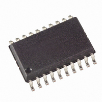
ATTINY2313V-10SJ Atmel, ATTINY2313V-10SJ Datasheet - Page 52

ATTINY2313V-10SJ
Manufacturer Part Number
ATTINY2313V-10SJ
Description
IC MCU AVR 2K FLASH 20SOIC
Manufacturer
Atmel
Series
AVR® ATtinyr
Specifications of ATTINY2313V-10SJ
Core Processor
AVR
Core Size
8-Bit
Speed
10MHz
Connectivity
SPI, UART/USART
Peripherals
Brown-out Detect/Reset, POR, PWM, WDT
Number Of I /o
18
Program Memory Size
2KB (1K x 16)
Program Memory Type
FLASH
Eeprom Size
128 x 8
Ram Size
128 x 8
Voltage - Supply (vcc/vdd)
1.8 V ~ 5.5 V
Oscillator Type
Internal
Operating Temperature
-40°C ~ 85°C
Package / Case
20-SOIC (7.5mm Width)
Lead Free Status / RoHS Status
Lead free / RoHS Compliant
Data Converters
-
Other names
ATTINY2313V-12SJ
ATTINY2313V-12SJ
ATTINY2313V-12SJ
- Current page: 52 of 226
- Download datasheet (4Mb)
52
ATtiny2313
Table 23. Generic Description of Overriding Signals for Alternate Functions
The following subsections shortly describe the alternate functions for each port, and relate the
overriding signals to the alternate function. Refer to the alternate function description for further
details.
Signal Name
PUOE
PUOV
DDOE
DDOV
PVOE
PVOV
PTOE
DIEOE
DIEOV
DI
AIO
Full Name
Pull-up Override
Enable
Pull-up Override
Value
Data Direction
Override Enable
Data Direction
Override Value
Port Value
Override Enable
Port Value
Override Value
Port Toggle
Override Enable
Digital Input
Enable Override
Enable
Digital Input
Enable Override
Value
Digital Input
Analog
Input/Output
Description
If this signal is set, the pull-up enable is controlled by the
PUOV signal. If this signal is cleared, the pull-up is
enabled when {DDxn, PORTxn, PUD} = 0b010.
If PUOE is set, the pull-up is enabled/disabled when
PUOV is set/cleared, regardless of the setting of the
DDxn, PORTxn, and PUD Register bits.
If this signal is set, the Output Driver Enable is controlled
by the DDOV signal. If this signal is cleared, the Output
driver is enabled by the DDxn Register bit.
If DDOE is set, the Output Driver is enabled/disabled
when DDOV is set/cleared, regardless of the setting of
the DDxn Register bit.
If this signal is set and the Output Driver is enabled, the
port value is controlled by the PVOV signal. If PVOE is
cleared, and the Output Driver is enabled, the port Value
is controlled by the PORTxn Register bit.
If PVOE is set, the port value is set to PVOV, regardless
of the setting of the PORTxn Register bit.
If PTOE is set, the PORTxn Register bit is inverted.
If this bit is set, the Digital Input Enable is controlled by
the DIEOV signal. If this signal is cleared, the Digital Input
Enable is determined by MCU state (Normal mode, sleep
mode).
If DIEOE is set, the Digital Input is enabled/disabled when
DIEOV is set/cleared, regardless of the MCU state
(Normal mode, sleep mode).
This is the Digital Input to alternate functions. In the
figure, the signal is connected to the output of the schmitt
trigger but before the synchronizer. Unless the Digital
Input is used as a clock source, the module with the
alternate function will use its own synchronizer.
This is the Analog Input/output to/from alternate
functions. The signal is connected directly to the pad, and
can be used bi-directionally.
2543L–AVR–08/10
Related parts for ATTINY2313V-10SJ
Image
Part Number
Description
Manufacturer
Datasheet
Request
R

Part Number:
Description:
IC MCU AVR 2K FLASH 20DIP
Manufacturer:
Atmel
Datasheet:

Part Number:
Description:
IC MCU AVR 2K FLASH 20SOIC
Manufacturer:
Atmel
Datasheet:

Part Number:
Description:
Manufacturer:
Atmel Corporation
Datasheet:

Part Number:
Description:
Manufacturer:
ATMEL Corporation
Datasheet:

Part Number:
Description:
IC MCU AVR 2K FLASH 20MLF
Manufacturer:
Atmel
Datasheet:

Part Number:
Description:
IC MCU AVR 2K FLASH 20DIP
Manufacturer:
Atmel
Datasheet:

Part Number:
Description:
IC MCU AVR 2K FLASH 20SOIC
Manufacturer:
Atmel
Datasheet:

Part Number:
Description:
IC MCU AVR 2K FLASH 20DIP
Manufacturer:
Atmel
Datasheet:

Part Number:
Description:
IC MCU AVR 2K FLASH 20SOIC
Manufacturer:
Atmel
Datasheet:

Part Number:
Description:
IC MCU AVR 2K FLASH 20SOIC
Manufacturer:
Atmel
Datasheet:

Part Number:
Description:
IC MCU AVR 2K FLASH 20WQFN
Manufacturer:
Atmel
Datasheet:

Part Number:
Description:
8-bit AVR Microcontroller with 2K Bytes In-System Programmable Flash
Manufacturer:
ATMEL Corporation
Datasheet:

Part Number:
Description:
Attiny2313 8-bit With 2k Bytes Of In-system Programmable Flash
Manufacturer:
ATMEL Corporation
Datasheet:


