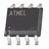
ATTINY12-8SI Atmel, ATTINY12-8SI Datasheet - Page 38

ATTINY12-8SI
Manufacturer Part Number
ATTINY12-8SI
Description
IC AVR MCU 1K 5V 8MHZ IND SO-8
Manufacturer
Atmel
Series
AVR® ATtinyr
Specifications of ATTINY12-8SI
Core Processor
AVR
Core Size
8-Bit
Speed
8MHz
Peripherals
POR, WDT
Number Of I /o
6
Program Memory Size
1KB (512 x 16)
Program Memory Type
FLASH
Eeprom Size
64 x 8
Voltage - Supply (vcc/vdd)
4 V ~ 5.5 V
Oscillator Type
Internal
Operating Temperature
-40°C ~ 85°C
Package / Case
8-SOIC (5.3mm Width), 8-SOP, 8-SOEIAJ
Data Bus Width
8 bit
Maximum Clock Frequency
8 MHz
Number Of Programmable I/os
12
Number Of Timers
1 x 8 bit
Operating Supply Voltage
4 V to 5.5 V
Maximum Operating Temperature
+ 85 C
Mounting Style
SMD/SMT
Minimum Operating Temperature
- 55 C
Lead Free Status / RoHS Status
Contains lead / RoHS non-compliant
Ram Size
-
Data Converters
-
Connectivity
-
Lead Free Status / Rohs Status
No
Other names
ATTINY128SI
Available stocks
Company
Part Number
Manufacturer
Quantity
Price
Company:
Part Number:
ATTINY12-8SI
Manufacturer:
ATMEL
Quantity:
1 729
Alternate Functions of Port B
All port B pins are connected to a pin change detector that can trigger the pin change
interrupt. See “Pin Change Interrupt” on page 32 for details. In addition, Port B has the
following alternate functions:
• RESET - Port B, Bit 5
When the RSTDISBL fuse is unprogrammed, this pin serves as external reset. When
the RSTDISBL fuse is programmed, this pin is a general input pin. In ATtiny12, it is also
an open-drain output pin.
• XTAL2 - Port B, Bit 4
XTAL2, oscillator output. When this pin is not used for clock purposes, it is a general I/O
pin. Refer to section “Pin Descriptions” on page 5 for details.
• XTAL1 - Port B, Bit 3
XTAL1, oscillator or clock input. When this pin is not used for clock purposes, it is a gen-
eral I/O pin. Refer to section “Pin Descriptions” on page 5 for details.
• T0/SCK - Port B, Bit 2
This pin can serve as the external counter clock input. See the timer/counter description
for further details. If external timer/counter clocking is selected, activity on this pin will
clock the counter even if it is configured as an output. In ATtiny12 and serial program-
ming mode, this pin serves as the serial clock input, SCK.
• INT0/AIN1/MISO - Port B, Bit 1
This pin can serve as the external interrupt0 input. See the interrupt description for
details on how to enable this interrupt. Note that activity on this pin will trigger the inter-
rupt even if the pin is configured as an output. This pin also serves as the negative input
of the on-chip Analog Comparator. In ATtiny12 and serial programming mode, this pin
serves as the serial data input, MISO.
• AIN0/MOSI - Port B, Bit 0
This pin also serves as the positive input of the on-chip Analog Comparator. In ATtiny12
and serial programming mode, this pin serves as the serial data output, MOSI.
During Power-down Mode, the schmitt triggers of the digital inputs are disconnected on
the Analog Comparator input pins. This allows an analog voltage close to V
/2 to be
CC
present during power-down without causing excessive power consumption.
ATtiny11/12
38
1006F–AVR–06/07


