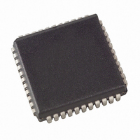
AT89C51RC-24JC Atmel, AT89C51RC-24JC Datasheet - Page 5

AT89C51RC-24JC
Manufacturer Part Number
AT89C51RC-24JC
Description
IC MICRO CTRL 24MHZ 44PLCC
Manufacturer
Atmel
Series
89Cr
Datasheet
1.AT89C51RC-24PU.pdf
(36 pages)
Specifications of AT89C51RC-24JC
Core Processor
8051
Core Size
8-Bit
Speed
24MHz
Connectivity
SPI, UART/USART
Peripherals
WDT
Number Of I /o
32
Program Memory Size
32KB (32K x 8)
Program Memory Type
FLASH
Ram Size
512 x 8
Voltage - Supply (vcc/vdd)
4 V ~ 5.5 V
Oscillator Type
Internal
Operating Temperature
0°C ~ 70°C
Package / Case
44-PLCC
For Use With
AT89STK-11 - KIT STARTER FOR AT89C51RX2
Lead Free Status / RoHS Status
Contains lead / RoHS non-compliant
Eeprom Size
-
Data Converters
-
Other names
AT89C51RC24JC
Available stocks
Company
Part Number
Manufacturer
Quantity
Price
4.6
4.7
4.8
4.9
1920D–MICRO–6/08
Port 3
RST
ALE/PROG
PSEN
Port 3 is an 8-bit bi-directional I/O port with internal pull-ups. The Port 3 output buffers can
sink/source four TTL inputs. When 1s are written to Port 3 pins, they are pulled high by the inter-
nal pull-ups and can be used as inputs. As inputs, Port 3 pins that are externally being pulled low
will source current (I
Port 3 receives some control signals for Flash programming and verification.
Port 3 also serves the functions of various special features of the AT89C51RC, as shown in the
following table.
Reset input. A high on this pin for two machine cycles while the oscillator is running resets the
device. This pin drives High for 98 oscillator periods after the Watchdog times out. The DISRTO
bit in SFR AUXR (address 8EH) can be used to disable this feature. In the default state of bit
DISRTO, the RESET HIGH out feature is enabled.
Address Latch Enable is an output pulse for latching the low byte of the address during
accesses to external memory. This pin is also the program pulse input (PROG) during Flash
programming.
In normal operation, ALE is emitted at a constant rate of 1/6 the oscillator frequency and may be
used for external timing or clocking purposes. Note, however, that one ALE pulse is skipped dur-
ing each access to external data memory.
If desired, ALE operation can be disabled by setting bit 0 of SFR location 8EH. With the bit set,
ALE is active only during a MOVX or MOVC instruction. Otherwise, the pin is weakly pulled high.
Setting the ALE-disable bit has no effect if the microcontroller is in external execution mode.
Program Store Enable is the read strobe to external program memory.
When the AT89C51RC is executing code from external program memory, PSEN is activated
twice each machine cycle, except that two PSEN activations are skipped during each access to
external data memory.
Port Pin
P3.0
P3.1
P3.2
P3.3
P3.4
P3.5
P3.6
P3.7
IL
) because of the pull-ups.
Alternate Functions
RXD (serial input port)
TXD (serial output port)
INT0 (external interrupt 0)
INT1 (external interrupt 1)
T0 (timer 0 external input)
T1 (timer 1 external input)
WR (external data memory write strobe)
RD (external data memory read strobe)
AT89C51RC
5


