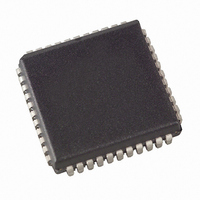
AT90S8515-8JI Atmel, AT90S8515-8JI Datasheet - Page 36

AT90S8515-8JI
Manufacturer Part Number
AT90S8515-8JI
Description
IC MCU 8K FLSH 8MHZ IT 44PLCC
Manufacturer
Atmel
Series
AVR® 90Sr
Datasheets
1.AT90S8515-4AC.pdf
(112 pages)
2.AT90S8515-4AC.pdf
(4 pages)
3.AT90S8515-4AC.pdf
(4 pages)
Specifications of AT90S8515-8JI
Core Processor
AVR
Core Size
8-Bit
Speed
8MHz
Connectivity
SPI, UART/USART
Peripherals
Brown-out Detect/Reset, POR, PWM, WDT
Number Of I /o
32
Program Memory Size
8KB (4K x 16)
Program Memory Type
FLASH
Eeprom Size
512 x 8
Ram Size
512 x 8
Voltage - Supply (vcc/vdd)
4 V ~ 6 V
Oscillator Type
Internal
Operating Temperature
-40°C ~ 85°C
Package / Case
44-PLCC
Lead Free Status / RoHS Status
Contains lead / RoHS non-compliant
Data Converters
-
Available stocks
Company
Part Number
Manufacturer
Quantity
Price
Company:
Part Number:
AT90S8515-8JI
Manufacturer:
ATM
Quantity:
4 500
Company:
Part Number:
AT90S8515-8JI
Manufacturer:
ATM
Quantity:
4 500
Part Number:
AT90S8515-8JI
Manufacturer:
ATMEL/爱特梅尔
Quantity:
20 000
Timer/Counter1 Control
Register A – TCCR1A
36
AT90S8515
• Bits 7, 6 – COM1A1, COM1A0: Compare Output Mode1A, Bits 1 and 0
The COM1A1 and COM1A0 control bits determine any output pin action following a
compare match in Timer/Counter1. Any output pin actions affect pin OC1A (Output
C o m p a r e A p i n 1 ) . T h i s i s a n a l t e r n a t i v e f u n c t i o n t o a n I / O p o r t a n d t h e
corresponding direction control bit must be set (one) to control the output pin. The con-
trol configuration is shown in Table 8.
• Bits 5, 4 – COM1B1, COM1B0: Compare Output Mode1B, Bits 1 and 0
The COM1B1 and COM1B0 control bits determine any output pin action following a
compare match in Timer/Counter1. Any output pin actions affect pin OC1B (Output
CompareB). The control configuration is given in Table 8.
Table 8. Compare 1 Mode Select
Note:
• Bits 3..2 – Res: Reserved Bits
These bits are reserved bits in the AT90S8515 and always read zero.
• Bits 1..0 – PWM11, PWM10: Pulse Width Modulator Select Bits 1 and 0
These bits select PWM operation of Timer/Counter1 as specified in Table 9. This mode
is described on page 40.
Table 9. PWM Mode Select
Bit
$2F ($4F)
Read/Write
Initial Value
COM1X1
PWM11
0
0
1
1
0
0
1
1
X = A or B
In PWM mode, these bits have a different function. Refer to Table 12 on page 40 for a
detailed description.
COM1A1
R/W
7
0
COM1X0
PWM10
0
1
0
1
0
1
0
1
COM1A0
R/W
6
0
Description
Timer/Counter1 disconnected from output pin OC1X
Toggle the OC1X output line.
Clear the OC1X output line (to zero).
Set the OC1X output line (to one).
Description
PWM operation of Timer/Counter1 is disabled
Timer/Counter1 is an 8-bit PWM
Timer/Counter1 is a 9-bit PWM
Timer/Counter1 is a 10-bit PWM
COM1B1
R/W
5
0
COM1B0
R/W
4
0
R
3
–
0
R
2
–
0
PWM11
R/W
1
0
PWM10
R/W
0
0
0841G–09/01
TCCR1A


