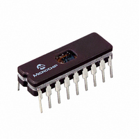
PIC16C715/JW Microchip Technology, PIC16C715/JW Datasheet - Page 28

PIC16C715/JW
Manufacturer Part Number
PIC16C715/JW
Description
IC MCU EPROM 2KX14 A/D 18CDIP
Manufacturer
Microchip Technology
Series
PIC® 16Cr
Specifications of PIC16C715/JW
Core Processor
PIC
Core Size
8-Bit
Speed
20MHz
Peripherals
Brown-out Detect/Reset, POR, WDT
Number Of I /o
13
Program Memory Size
3.5KB (2K x 14)
Program Memory Type
EPROM, UV
Ram Size
128 x 8
Voltage - Supply (vcc/vdd)
4 V ~ 5.5 V
Data Converters
A/D 4x8b
Oscillator Type
External
Operating Temperature
0°C ~ 70°C
Package / Case
18-CDIP (0.300", 7.62mm) Window
Lead Free Status / RoHS Status
Contains lead / RoHS non-compliant
Eeprom Size
-
Connectivity
-
Available stocks
Company
Part Number
Manufacturer
Quantity
Price
- Current page: 28 of 177
- Download datasheet (2Mb)
PIC16C71X
FIGURE 5-4:
TABLE 5-3:
DS30272A-page 28
Set RBIF
Name
RB0/INT
RB7
Legend: TTL = TTL input, ST = Schmitt Trigger input
Note 1: This buffer is a Schmitt Trigger input when configured as the external interrupt.
RB1
RB2
RB3
RB4
RB5
RB6
Data bus
WR TRIS
WR Port
RBPU
RB7:RB6 in serial programming mode
Note 1: I/O pins have diode protection to V
2: This buffer is a Schmitt Trigger input when used in serial programming mode.
2: TRISB = ’1’ enables weak pull-up if
(2)
From other
RB7:RB4 pins
RBPU = ’0’ (OPTION<7>).
Bit#
bit0
bit1
bit2
bit3
bit4
bit5
bit6
bit7
BLOCK DIAGRAM OF
RB7:RB4 PINS
(PIC16C71)
PORTB FUNCTIONS
RD TRIS
RD Port
Data Latch
TRIS Latch
D
D
CK
CK
Q
Q
TTL/ST
TTL/ST
TTL/ST
Buffer
TTL
TTL
TTL
TTL
TTL
Q
Q
Latch
(1)
(2)
(2)
DD
EN
EN
D
D
TTL
Input
Buffer
and V
Function
Input/output pin or external interrupt input. Internal software
programmable weak pull-up.
Input/output pin. Internal software programmable weak pull-up.
Input/output pin. Internal software programmable weak pull-up.
Input/output pin. Internal software programmable weak pull-up.
Input/output pin (with interrupt on change). Internal software programmable
weak pull-up.
Input/output pin (with interrupt on change). Internal software programmable
weak pull-up.
Input/output pin (with interrupt on change). Internal software programmable
weak pull-up. Serial programming clock.
Input/output pin (with interrupt on change). Internal software programmable
weak pull-up. Serial programming data.
V
RD Port
SS
P
DD
.
Buffer
weak
pull-up
I/O
pin
ST
(1)
FIGURE 5-5:
Data bus
WR Port
WR TRIS
RBPU
RB7:RB6 in serial programming mode
Set RBIF
Note 1: I/O pins have diode protection to V
From other
RB7:RB4 pins
2: TRISB = ’1’ enables weak pull-up if
(2)
RBPU = ’0’ (OPTION<7>).
RD TRIS
RD Port
Data Latch
TRIS Latch
D
D
BLOCK DIAGRAM OF
RB7:RB4 PINS
(PIC16C710/711/715)
CK
CK
Q
Q
1997 Microchip Technology Inc.
Q
Q
Latch
DD
EN
EN
D
D
TTL
Input
Buffer
and V
V
P
SS
DD
.
weak
pull-up
RD Port
Buffer
I/O
pin
Q1
Q3
(1)
ST
Related parts for PIC16C715/JW
Image
Part Number
Description
Manufacturer
Datasheet
Request
R

Part Number:
Description:
IC MCU EPROM 1KX14 A/D 18CDIP
Manufacturer:
Microchip Technology
Datasheet:

Part Number:
Description:
IC MCU OTP 1KX14 A/D 18DIP
Manufacturer:
Microchip Technology
Datasheet:

Part Number:
Description:
IC MCU OTP 1KX14 A/D 18SOIC
Manufacturer:
Microchip Technology
Datasheet:

Part Number:
Description:
IC MCU OTP 1KX14 A/D 18DIP
Manufacturer:
Microchip Technology
Datasheet:

Part Number:
Description:
IC MCU OTP 1KX14 A/D 18DIP
Manufacturer:
Microchip Technology
Datasheet:

Part Number:
Description:
IC MCU OTP 1KX14 A/D 18SOIC
Manufacturer:
Microchip Technology
Datasheet:

Part Number:
Description:
IC MCU OTP 1KX14 A/D 18SOIC
Manufacturer:
Microchip Technology
Datasheet:

Part Number:
Description:
IC MCU OTP 1KX14 A/D 18SOIC
Manufacturer:
Microchip Technology
Datasheet:

Part Number:
Description:
IC MCU OTP 1KX14 A/D 18DIP
Manufacturer:
Microchip Technology
Datasheet:

Part Number:
Description:
8-Bit CMOS Microcontrollers with A/D Converter
Manufacturer:
Microchip Technology
Datasheet:

Part Number:
Description:
8-Bit CMOS Microcontrollers with A/D Converter
Manufacturer:
Microchip Technology

Part Number:
Description:
8-Bit CMOS Microcontrollers with A/D Converter
Manufacturer:
Microchip Technology

Part Number:
Description:
8-Bit CMOS Microcontrollers with A/D Converter
Manufacturer:
Microchip Technology

Part Number:
Description:
8-Bit CMOS Microcontrollers with A/D Converter
Manufacturer:
Microchip Technology

Part Number:
Description:
8-Bit CMOS Microcontrollers with A/D Converter
Manufacturer:
Microchip Technology


