PIC16C62A/JW Microchip Technology, PIC16C62A/JW Datasheet
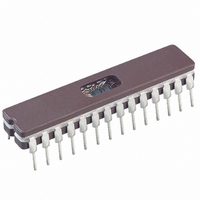
IC MCU EPROM 2KX14 PWM 28CDIP

PIC16C62A/JW

Manufacturer Part Number
PIC16C62A/JW
Description
IC MCU EPROM 2KX14 PWM 28CDIP
Manufacturer
Microchip Technology
Series
PIC® 16Cr

Specifications of PIC16C62A/JW

Core Processor
PIC
Core Size
8-Bit
Speed
20MHz
Connectivity
I²C, SPI
Peripherals
Brown-out Detect/Reset, POR, PWM, WDT
Number Of I /o
22
Program Memory Size
3.5KB (2K x 14)
Program Memory Type
EPROM, UV
Ram Size
128 x 8
Voltage - Supply (vcc/vdd)
4 V ~ 6 V
Oscillator Type
External
Operating Temperature
0°C ~ 70°C
Package / Case
28-CDIP (0.300", 7.62mm) Window
Lead Free Status / RoHS Status
Contains lead / RoHS non-compliant
Eeprom Size
-
Data Converters
-

Available stocks

Company
Part Number
Manufacturer
Quantity
Price
Part Number:
PIC16C62A/JW
Manufacturer:
MICROCHIP
Quantity:
330
Part Number:
PIC16C62A/JW
Manufacturer:
MICROCHIP
Quantity:
1 000
The PIC16C62A (Rev. A) parts you have received con-
form
(DS30234D), except for the anomalies described
below.
All the problems listed here will be addressed in future
revisions of the PIC16C62A silicon.
1. Module: CCP (Compare Mode)
TABLE 1:
 2001 Microchip Technology Inc.
CCPxM<3:0> =
CCP Mode
The Compare mode may not operate as expected
when configuring the compare match to drive the
I/O pin low (CCPxM<3:0> = 1001).
When the CCP module is changed to compare
output low (CCPxM<3:0> = 1001) from any other
non-compare CCP mode, the I/O pin will immedi-
ately be driven low, regardless of the state of the
I/O data latch. The pin will remain low when the
compare match occurs (see Table 1).
However, when the CCP module is changed to
compare output high (CCPxM<3:0> = 1000) from
any other CCP mode, the I/O pin will immediately
be driven low, regardless of the state of the I/O
data latch. The pin will be driven high when the
compare match occurs.
functionally
0xxx
1000
1001
101x
11xx
COMPARE OUTPUT LOW
SWITCHING
PIC16C62A Rev. A Silicon Errata Sheet
to
I/O pin
State
H
H
H
H
H
L
L
L
L
L
the
Device
1001
Change CCP to
CCPxM<3:0> =
H
L
L
L
L
L
L
L
Data
1000
Sheet
L
L
L
L
L
L
L
L
2. Module: CCP (Compare Mode)
3. Module: SSP Module (I
Work around
To have the I/O pin high until the compare match
low occurs, force a compare match high to get the
I/O pin into the high state, then reconfigure the
compare match to force the I/O low, when the com-
pare condition occurs.
The special event trigger of the Compare mode
may not occur if both of the following conditions
exist:
CCP1
The interrupt for the compare event will still be
generated, but no special event trigger will occur.
Work around
Use the Interrupt Service Routine instead of using
the special event trigger to reset Timer1 (and start
an A/D conversion, if applicable).
If the bus is active when the I
and the next 8 bits of data on the bus match the
address of the device, then the SSP module will
generate an Acknowledge pulse.
Work around
Before enabling the I
is not active.
Unit
PIC16C62A
An instruction, one cycle (T
Timer1/Compare register match has literal
data equal to the address of a CCP register
being used. Specific cases include:
An instruction in the same cycle as a
Timer1/Compare register match has an
MSb of ‘0’.
CCP1CON
Register
CCPR1H
CCPR1L
2
C mode, ensure that the bus
2
C™ mode)
2
C mode is enabled,
CY
) prior to a
DS80093A-page 1
Literal Data
15h
16h
17h

Related parts for PIC16C62A/JW

PIC16C62A/JW Summary of contents

Page 1

... 11xx L L  2001 Microchip Technology Inc. PIC16C62A Work around Data Sheet To have the I/O pin high until the compare match low occurs, force a compare match high to get the I/O pin into the high state, then reconfigure the compare match to force the I/O low, when the com- pare condition occurs ...

Page 2

... TMR1H:TMR1L = 00:00 (TMR1IF is not set.) Work around To preserve Timer1 register values: a) Read Timer1 register values into “shadow” registers. b) Perform any write instruction(s) on the shadow registers. c) Write the shadow register values back into the Timer1 registers.  2001 Microchip Technology Inc. ...

Page 3

... Last clock edge of the Byte1 to 1st 73A clock edge of the Byte2 * This parameter is characterized but not tested. Note 1: Specification 73A is only required if specifications 71A and 72A are used.  2001 Microchip Technology Inc. New Specification Min Typ Max — — 10 New Specification ...

Page 4

... Timer1 oscillator components, and exter- nal clock frequency, the Timer1 increment clock may not 50% duty cycle. The TMR1 increment clock is out of phase of the T1OSO/T1CKI pin by a small propagation delay. Write to TMR1H and/or TMR1L Register(s) TMR1H:TMR1L Increments  2001 Microchip Technology Inc. IH ...

Page 5

... Table 4. TABLE 4: MINIMUM AND MAXIMUM BOR RESET VOLTAGES Param Sym. Characteristic No. D005 V Brown-out Reset Voltage BOR  2001 Microchip Technology Inc. Correct Characterization Data Average % Variation 3.55 MHz ± 9.63% 1.99 MHz ± 10.53% 221.9 kHz ± 12.10% 1.77 MHz ± ...

Page 6

... PIC16C62A NOTES: DS80093A-page 6  2001 Microchip Technology Inc. ...

Page 7

... L , SEEVAL, MPLAB and The EE OQ Embedded Control Solutions Company are registered trade- marks of Microchip Technology Incorporated in the U.S.A. and other countries. Total Endurance, ICSP, In-Circuit Serial Programming, Filter- Lab, MXDEV, microID, FlexROM, fuzzyLAB, MPASM, MPLINK, MPLIB, PICDEM, ICEPIC, Migratable Memory, FanSense, ECONOMONITOR, SelectMode and microPort are trademarks of Microchip Technology Incorporated in the U ...

Page 8

... Microchip. No licenses are conveyed, implicitly or otherwise, except as maybe explicitly expressed herein, under any intellec- tual property rights. The Microchip logo and name are registered trademarks of Microchip Technology Inc. in the U.S.A. and other countries. All rights reserved. All other trademarks mentioned herein are the property of their respective companies. ...

Related keywords