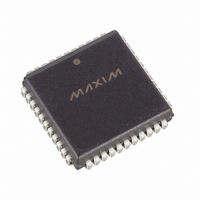
DS89C450-QNL+ Maxim Integrated Products, DS89C450-QNL+ Datasheet - Page 23

DS89C450-QNL+
Manufacturer Part Number
DS89C450-QNL+
Description
IC MCU FLASH 64KB 33MHZ 44-PLCC
Manufacturer
Maxim Integrated Products
Series
89Cr
Datasheet
1.DS89C450-KIT.pdf
(46 pages)
Specifications of DS89C450-QNL+
Core Processor
8051
Core Size
8-Bit
Speed
33MHz
Connectivity
EBI/EMI, SIO, UART/USART
Peripherals
Power-Fail Reset, WDT
Number Of I /o
32
Program Memory Size
64KB (64K x 8)
Program Memory Type
FLASH
Ram Size
1K x 8
Voltage - Supply (vcc/vdd)
4.5 V ~ 5.5 V
Oscillator Type
External
Operating Temperature
-40°C ~ 85°C
Package / Case
44-LCC, 44-PLCC
Processor Series
89C
Core
8051
Data Bus Width
8 bit
Data Ram Size
1 KB
Maximum Clock Frequency
33 MHz
Number Of Programmable I/os
32
Number Of Timers
3
Operating Supply Voltage
5 V
Maximum Operating Temperature
+ 85 C
Mounting Style
SMD/SMT
3rd Party Development Tools
PK51, CA51, A51, ULINK2
Development Tools By Supplier
DS89C450-K00
Minimum Operating Temperature
- 40 C
Interface Type
UART
Lead Free Status / RoHS Status
Lead free / RoHS Compliant
Eeprom Size
-
Data Converters
-
Lead Free Status / Rohs Status
Lead free / RoHS Compliant
The signature bytes can be read in ROM loader mode or in parallel programming mode. Reading data from
addresses 30h, 31h, and 60h provides signature information on manufacturer, part, and extension as follows:
Note: The read/write accessibility of the flash memory during in-application programming is not affected by the state of the lock
bits. However, the lock bits do affect the read/write accessibility in ROM loader and parallel programming modes.
In-Application Programming by User Software
The DS89C430 supports in-application programming of on-chip flash memory by user software. In-application
programming is initiated by writing a flash command into the flash control (FCNTL:D5h) register to enable the flash
memory for erase/program/verify operations. Address and data are input into the MMU through the flash data
(FDATA:D6h) register. The flash command also enables read/write accesses to the FDATA. The MMU’s sequencer
provides the operation sequences and control functions to the flash memory. The MMU is designed to operate
independently from the processor, except for read/write access to the SFRs.
Only the upper bank of the on-chip program memory can be in-application programmed by the user software. The
lower bank of the on-chip program memory contains system hardware-dependent codes that are crucial to system
operation and should not be altered during in-application programming.
All flash operations are self-timed. The user software can monitor the progress of an erase or programming
operation through the flash busy (FBUSY;FCNTL.7) bit with a reset value at logic 1. A selected operation
automatically starts when required data is written to the FDATA SFR. The MMU clears the FBUSY bit to indicate
the start of a write/erase operation. The FBUSY bit may not change state for up to 1s after the operation is
requested. During this time, the application should poll the status of the FBUSY bit waiting for it to change state.
This bit is held low until either the end of the operation or until an error indicator is returned. A flash operating
failure terminates the current operation and sets the flash error flag (FERR;FCNTL.6) to logic 1. Both the busy and
error flags are read-only bits.
Read/write access during in-application programming is not affected by the state of the lock bits.
A sample programming sequence for a "w
reentered each time an operation is requested, i.e., it is not permissible to issue the “write upper program memory
bank” command once and then repeatedly load address and data values to program a block of memory.
1. Make sure the FBUSY bit is 1 to indicate flash MMU is idle.
2. Write 0Bh to the FCNTL register using the timed access sequence.
3. Write address_MSB to the FDATA register.
4. Write address_LSB to the FDATA register.
5. Write data_value to the FDATA register.
6. Make sure the FBUSY bit is 0 to indicate programming has started.
7. Wait for FBUSY bit to return to 1 to indicate end of programming operation.
8. Make sure FERR is 0 to indicate no programming error.
The flash command (FC3–FC0;FCNTL.3:0) bits provide flash commands as listed in
ADDRESS
30h
31h
31h
31h
60h
VALUE
DAh
43h
44h
45h
01h
Manufacturer ID
DS89C430 Device ID
DS89C440 Device ID (Contact factory or replace with DS89C430 or DS89C450.)
DS89C450 Device ID
Device Extension
rite upper program memory bank
DS89C430/DS89C450 Ultra-High-Speed Flash Microcontrollers
23 of 46
MEANING
" is shown below. The command must be
Table
4.


