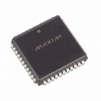
DS89C450-QNG+ Maxim Integrated Products, DS89C450-QNG+ Datasheet - Page 26

DS89C450-QNG+
Manufacturer Part Number
DS89C450-QNG+
Description
IC MCU FLASH 64KB 25MHZ 44-PLCC
Manufacturer
Maxim Integrated Products
Series
89Cr
Datasheet
1.DS89C450-KIT.pdf
(46 pages)
Specifications of DS89C450-QNG+
Core Processor
8051
Core Size
8-Bit
Speed
25MHz
Connectivity
EBI/EMI, SIO, UART/USART
Peripherals
Power-Fail Reset, WDT
Number Of I /o
32
Program Memory Size
64KB (64K x 8)
Program Memory Type
FLASH
Ram Size
1K x 8
Voltage - Supply (vcc/vdd)
4.5 V ~ 5.5 V
Oscillator Type
External
Operating Temperature
-40°C ~ 85°C
Package / Case
44-LCC, 44-PLCC
Processor Series
DS89C450
Core
8051
Data Bus Width
8 bit
Data Ram Size
1 KB
Interface Type
UART
Maximum Clock Frequency
33 MHz
Number Of Programmable I/os
4
Number Of Timers
3
Operating Supply Voltage
4.5 V to 5.5 V
Maximum Operating Temperature
+ 85 C
Mounting Style
SMD/SMT
3rd Party Development Tools
PK51, CA51, A51, ULINK2
Development Tools By Supplier
DS89C450-KIT#
Minimum Operating Temperature
- 40 C
Lead Free Status / RoHS Status
Lead free / RoHS Compliant
Eeprom Size
-
Data Converters
-
Lead Free Status / Rohs Status
Details
External Memory
The DS89C430 executes external memory cycles for code fetches and read/writes of external program and data
memory. A nonpage external memory cycle is four times slower than the internal memory cycles (i.e., an external
memory cycle contains four system clocks). However, a page mode external memory cycle can be completed in
one, two, or four system clocks for a page hit and two, four, or eight system clocks for a page miss, depending on
user selection. The DS89C430 also supports a second page mode operation with a different external bus structure
that provides for fast external code fetches but uses four system clock cycles for data memory access.
External Program Memory Interface (Nonpage Mode)
Figure 7
assuming the microcontroller is in nonpage mode for external fetches. Note that an external program fetch takes
four system clocks, and an internal program fetch requires only one system clock.
As illustrated in
programmable user option to turn on ALE during internal program memory operation. ALE is automatically enabled
for code fetch externally, independent of the setting of this option.
PSEN is only asserted for external code fetches, and is inactive during internal execution.
Figure 7. External Program Memory Access (Nonpage Mode, CD1:CD0 = 10)
XTAL1
ALE
PSEN
Port 0
Port 2
shows the timing relationship for internal and external code fetches when CD1 and CD0 are set to 10b,
Internal Memory Cycles
Figure
7, ALE is deasserted when executing an internal memory fetch. The DS89C430 provides a
External Memory Cycle
C1
LSB Add
C2
DS89C430/DS89C450 Ultra-High-Speed Flash Microcontrollers
MSB Add
26 of 46
C3
C4
Data
External Memory Cycle
C1
LSB Add
C2
MSB Add
C3
Data
C4


