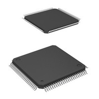
M30624FGNHP#U5 Renesas Electronics America, M30624FGNHP#U5 Datasheet - Page 25

M30624FGNHP#U5
Manufacturer Part Number
M30624FGNHP#U5
Description
MCU 3V 256K PB-FREE 100-TQFP
Manufacturer
Renesas Electronics America
Series
M16C™ M16C/60r
Datasheet
1.M30620FCNGPU5.pdf
(250 pages)
Specifications of M30624FGNHP#U5
Core Processor
M16C/60
Core Size
16-Bit
Speed
16MHz
Connectivity
SIO, UART/USART
Peripherals
DMA, PWM, WDT
Number Of I /o
85
Program Memory Size
256KB (256K x 8)
Program Memory Type
FLASH
Ram Size
20K x 8
Voltage - Supply (vcc/vdd)
3 V ~ 3.6 V
Data Converters
A/D 18x10b, D/A 2x8b
Oscillator Type
Internal
Operating Temperature
-20°C ~ 85°C
Package / Case
100-TQFP, 100-VQFP
Lead Free Status / RoHS Status
Lead free / RoHS Compliant
Eeprom Size
-
Available stocks
Company
Part Number
Manufacturer
Quantity
Price
- Current page: 25 of 250
- Download datasheet (4Mb)
Memory Space Expansion Features
22
Figure 1.7.3. Memory location and chip select area in expansion mode 2
Figure 1.7.2. Data bank register
(2) Expansion mode
In expansion mode, the data bank register (0000B
register.
Note 1: These memory maps show an instance in which PM13 is set to 0; but in the case of products in which the internal
Note 2: The memory maps in single-chip mode are omitted.
XXXXX
YYYYY
FFFFF
10K bytes
12K bytes
D0000
20K bytes
Expansion mode (memory space = 4M bytes for PM15 = 1, PM14 = 1)
00000
00400
04000
08000
28000
40000
RAM size
Data bank register
b7
RAM and the internal ROM are expanded to over 15 Kbytes and 192 Kbytes, respectively, they show an instance
in which PM13 is set to 1.
16
16
16
16
16
16
16
16
16
16
b6
Internal area reserved
Internal area reserved
Internal ROM area
Internal RAM area
expansion mode
b5
External area
Address XXXXX
Memory
SFR area
b4
02BFF
033FF
053FF
b3
16
16
16
b2
b1
16
b0
Internal area reserved
Internal RAM area
Microprocessor
External area
128K bytes
256K bytes
ROM size
Bit symbol
SFR area
Nothing is assigned.
In an attempt to write to these bits, write “0”. The value, if read, turns out to be “0”.
Nothing is assigned.
In an attempt to write to these bits, write “0”. The value, if read, turns out to be “0”.
mode
BSR
OFS
Symbol
DBR
Address YYYYY
Bank selection bits
Offset bit
E0000
C0000
CS3
CS2
CS1
CS0
Memory expansion mode:
Microprocessor mode:
512K bytes x 7banks +
256K bytes
512K bytes x 8banks
(16K bytes)
(128K bytes)
(96K bytes)
Bit name
16
16
Address
000B
16
16
) goes effective. Figure 1.7.2 shows the data bank
16
SINGLE-CHIP 16-BIT CMOS MICROCOMPUTER
b5 b4 b3
When reset
Addresses from 40000
Addresses from C0000
Bank number is output to CS3 to CS1
0: Not offset
1: Offset
0 0 0: Bank 0
0 1 0: Bank 2
1 0 0: Bank 4
1 1 0: Bank 6
Bank 7 in fetching a program
A bank selected by use of the bank selection
bits in accessing data
Bank 7 invariably
00
16
Description
b5 b4 b3
0 0 1: Bank 1
0 1 1: Bank 3
1 0 1: Bank 5
1 1 1: Bank 7
16
16
through BFFFF
through FFFFF
M16C / 62N Group
Mitsubishi microcomputers
R
16
16
W
Related parts for M30624FGNHP#U5
Image
Part Number
Description
Manufacturer
Datasheet
Request
R

Part Number:
Description:
KIT STARTER FOR M16C/29
Manufacturer:
Renesas Electronics America
Datasheet:

Part Number:
Description:
KIT STARTER FOR R8C/2D
Manufacturer:
Renesas Electronics America
Datasheet:

Part Number:
Description:
R0K33062P STARTER KIT
Manufacturer:
Renesas Electronics America
Datasheet:

Part Number:
Description:
KIT STARTER FOR R8C/23 E8A
Manufacturer:
Renesas Electronics America
Datasheet:

Part Number:
Description:
KIT STARTER FOR R8C/25
Manufacturer:
Renesas Electronics America
Datasheet:

Part Number:
Description:
KIT STARTER H8S2456 SHARPE DSPLY
Manufacturer:
Renesas Electronics America
Datasheet:

Part Number:
Description:
KIT STARTER FOR R8C38C
Manufacturer:
Renesas Electronics America
Datasheet:

Part Number:
Description:
KIT STARTER FOR R8C35C
Manufacturer:
Renesas Electronics America
Datasheet:

Part Number:
Description:
KIT STARTER FOR R8CL3AC+LCD APPS
Manufacturer:
Renesas Electronics America
Datasheet:

Part Number:
Description:
KIT STARTER FOR RX610
Manufacturer:
Renesas Electronics America
Datasheet:

Part Number:
Description:
KIT STARTER FOR R32C/118
Manufacturer:
Renesas Electronics America
Datasheet:

Part Number:
Description:
KIT DEV RSK-R8C/26-29
Manufacturer:
Renesas Electronics America
Datasheet:

Part Number:
Description:
KIT STARTER FOR SH7124
Manufacturer:
Renesas Electronics America
Datasheet:

Part Number:
Description:
KIT STARTER FOR H8SX/1622
Manufacturer:
Renesas Electronics America
Datasheet:

Part Number:
Description:
KIT DEV FOR SH7203
Manufacturer:
Renesas Electronics America
Datasheet:


