MC908AZ60AVFUE Freescale Semiconductor, MC908AZ60AVFUE Datasheet - Page 338
MC908AZ60AVFUE
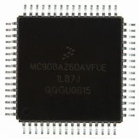
Manufacturer Part Number
MC908AZ60AVFUE
Description
IC MCU 61K FLASH 8.4MHZ 64-QFP
Manufacturer
Freescale Semiconductor
Series
HC08r
Datasheet
1.MC908AZ60ACFUER.pdf
(414 pages)
Specifications of MC908AZ60AVFUE
Core Processor
HC08
Core Size
8-Bit
Speed
8.4MHz
Connectivity
CAN, SCI, SPI
Peripherals
LVD, POR, PWM
Number Of I /o
52
Program Memory Size
60KB (60K x 8)
Program Memory Type
FLASH
Eeprom Size
1K x 8
Ram Size
2K x 8
Voltage - Supply (vcc/vdd)
4.5 V ~ 5.5 V
Data Converters
A/D 15x8b
Oscillator Type
Internal
Operating Temperature
-40°C ~ 105°C
Package / Case
64-QFP
Processor Series
HC08AZ
Core
HC08
Data Bus Width
8 bit
Data Ram Size
2 KB
Interface Type
SCI, SPI
Maximum Clock Frequency
8.4 MHz
Number Of Programmable I/os
52
Number Of Timers
8
Maximum Operating Temperature
+ 105 C
Mounting Style
SMD/SMT
Development Tools By Supplier
FSICEBASE, M68CBL05CE, ZK-HC08AX-A, M68EM08AS/AZ60AE
Minimum Operating Temperature
- 40 C
On-chip Adc
8 bit, 15 Channel
Lead Free Status / RoHS Status
Lead free / RoHS Compliant
Available stocks
Company
Part Number
Manufacturer
Quantity
Price
Company:

Part Number:
MC908AZ60AVFUE
Manufacturer:
FREESCALE
Quantity:
2 500
Company:
Part Number:
MC908AZ60AVFUE
Manufacturer:
Freescale Semiconductor
Quantity:
10 000
Part Number:
MC908AZ60AVFUE
Manufacturer:
FREESCALE
Quantity:
20 000
Company:
Part Number:
MC908AZ60AVFUER
Manufacturer:
Freescale Semiconductor
Quantity:
10 000


Byte Data Link Controller (BDLC)
27.3.1.3 Run Mode
This mode is entered from the reset mode after all MCU reset sources are no longer asserted. Run mode
is entered from the BDLC wait mode whenever activity is sensed on the J1850 bus.
Run mode is entered from the BDLC stop mode whenever network activity is sensed, although messages
will not be received properly until the clocks have stabilized and the CPU is in run mode also.
In this mode, normal network operation takes place. The user should ensure that all BDLC transmissions
have ceased before exiting this mode.
27.3.1.4 BDLC Wait Mode
This power-conserving mode is entered automatically from run mode whenever the CPU executes a
WAIT instruction and if the WCM bit in the BCR1 register is cleared previously.
In this mode, the BDLC internal clocks continue to run. The first passive-to-active transition of the bus
generates a CPU interrupt request from the BDLC which wakes up the BDLC and the CPU. In addition,
if the BDLC receives a valid EOF symbol while operating in wait mode, then the BDLC also will generate
a CPU interrupt request which wakes up the BDLC and the CPU. See
27.7.1 Wait
Mode.
27.3.1.5 BDLC Stop Mode
This power-conserving mode is entered automatically from run mode whenever the CPU executes a
STOP instruction or if the CPU executes a WAIT instruction and the WCM bit in the BCR1 register is set
previously.
In this mode, the BDLC internal clocks are stopped but the physical interface circuitry is placed in a
low-power mode and awaits network activity. If network activity is sensed, then a CPU interrupt request
will be generated, restarting the BDLC internal clocks. See
27.7.2 Stop
Mode.
27.3.1.6 Digital Loopback Mode
When a bus fault has been detected, the digital loopback mode is used to determine if the fault condition
is caused by failure in the node’s internal circuits or elsewhere in the network, including the node’s analog
physical interface. In this mode, the transmit digital output pin (BDTxD) and the receive digital input pin
(BDRxD) of the digital interface are disconnected from the analog physical interface and tied together to
allow the digital portion of the BDLC to transmit and receive its own messages without driving the J1850
bus.
27.3.1.7 Analog Loopback Mode
Analog loopback is used to determine if a bus fault has been caused by a failure in the node’s off-chip
analog transceiver or elsewhere in the network. The BCLD analog loopback mode does not modify the
digital transmit or receive functions of the BDLC. It does, however, ensure that once analog loopback
mode is exited, the BDLC will wait for an idle bus condition before participation in network communication
resumes. If the off-chip analog transceiver has a loopback mode, it usually causes the input to the output
drive stage to be looped back into the receiver, allowing the node to receive messages it has transmitted
without driving the J1850 bus. In this mode, the output to the J1850 bus is typically high impedance. This
allows the communication path through the analog transceiver to be tested without interfering with
network activity. Using the BDLC analog loopback mode in conjunction with the analog transceiver’s
loopback mode ensures that, once the off-chip analog transceiver has exited loopback mode, the BCLD
will not begin communicating before a known condition exists on the J1850 bus.
MC68HC908AZ60A • MC68HC908AS60A • MC68HC908AS60E Data Sheet, Rev. 6
338
Freescale Semiconductor
Related parts for MC908AZ60AVFUE
Image
Part Number
Description
Manufacturer
Datasheet
Request
R

Part Number:
Description:
Manufacturer:
Freescale Semiconductor, Inc
Datasheet:
Part Number:
Description:
Manufacturer:
Freescale Semiconductor, Inc
Datasheet:
Part Number:
Description:
Manufacturer:
Freescale Semiconductor, Inc
Datasheet:
Part Number:
Description:
Manufacturer:
Freescale Semiconductor, Inc
Datasheet:
Part Number:
Description:
Manufacturer:
Freescale Semiconductor, Inc
Datasheet:
Part Number:
Description:
Manufacturer:
Freescale Semiconductor, Inc
Datasheet:
Part Number:
Description:
Manufacturer:
Freescale Semiconductor, Inc
Datasheet:
Part Number:
Description:
Manufacturer:
Freescale Semiconductor, Inc
Datasheet:
Part Number:
Description:
Manufacturer:
Freescale Semiconductor, Inc
Datasheet:
Part Number:
Description:
Manufacturer:
Freescale Semiconductor, Inc
Datasheet:
Part Number:
Description:
Manufacturer:
Freescale Semiconductor, Inc
Datasheet:
Part Number:
Description:
Manufacturer:
Freescale Semiconductor, Inc
Datasheet:
Part Number:
Description:
Manufacturer:
Freescale Semiconductor, Inc
Datasheet:
Part Number:
Description:
Manufacturer:
Freescale Semiconductor, Inc
Datasheet:
Part Number:
Description:
Manufacturer:
Freescale Semiconductor, Inc
Datasheet: