COP8CCR9IMT7/NOPB National Semiconductor, COP8CCR9IMT7/NOPB Datasheet - Page 14
COP8CCR9IMT7/NOPB
Manufacturer Part Number
COP8CCR9IMT7/NOPB
Description
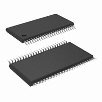
IC MCU EEPROM 8BIT 32K 48-TSSOP
Manufacturer
National Semiconductor
Series
COP8™ 8Cr
Datasheet
1.COP8CDR9HVA8NOPB.pdf
(84 pages)
Specifications of COP8CCR9IMT7/NOPB
Core Processor
COP8
Core Size
8-Bit
Speed
20MHz
Connectivity
Microwire/Plus (SPI), UART/USART
Peripherals
Brown-out Detect/Reset, POR, PWM, WDT
Number Of I /o
39
Program Memory Size
32KB (32K x 8)
Program Memory Type
FLASH
Ram Size
1K x 8
Voltage - Supply (vcc/vdd)
2.7 V ~ 5.5 V
Data Converters
A/D 16x10b
Oscillator Type
Internal
Operating Temperature
-40°C ~ 125°C
Package / Case
48-TSSOP
Data Bus Width
8 bit
Maximum Clock Frequency
20 MHz
Data Ram Size
1 KB
On-chip Adc
10 bit, 16 channel
Number Of Programmable I/os
59
Number Of Timers
3
Height
0.9 mm
Interface Type
SPI, USART
Length
12.5 mm
Maximum Operating Temperature
+ 125 C
Minimum Operating Temperature
- 40 C
Supply Voltage (max)
5.5 V
Supply Voltage (min)
4.5 V
Width
6.1 mm
Lead Free Status / RoHS Status
Lead free / RoHS Compliant
Eeprom Size
-
Lead Free Status / Rohs Status
Details
Other names
*COP8CCR9IMT7
*COP8CCR9IMT7/NOPB
COP8CCR9IMT7
*COP8CCR9IMT7/NOPB
COP8CCR9IMT7
Available stocks
Company
Part Number
Manufacturer
Quantity
Price
Company:

Part Number:
COP8CCR9IMT7/NOPB
Manufacturer:
NS/TI
Quantity:
8


www.national.com
8.0 Electrical Characteristics
AC Electrical Characteristics (−40˚C ≤ T
Resolution
DNL
DNL
INL
INL
Offset Error
Offset Error
Gain Error
Gain Error
Input Voltage Range
Analog Input Leakage Current
Analog Input Resistance (Note 9)
Analog Input Capacitance
Conversion Clock Period
Output Pulse Width
USART Bit Time when using External
CKX
USART CKX Frequency when being
Driven by Internal Baud Rate Generator
Reset Pulse Width
t
Note 2: Maximum rate of voltage change must be
Note 3: Supply and IDLE currents are measured with CKI driven with a square wave Oscillator, CKO driven 180˚ out of phase with CKI, inputs connected to V
and outputs driven low but not connected to a load.
Note 4: The HALT mode will stop CKI from oscillating. Measurement of I
and G2–G5 programmed as low outputs and not driving a load; all D outputs programmed low and not driving a load; all inputs tied to V
monitor and BOR disabled. Parameter refers to HALT mode entered via setting bit 7 of the G Port data register.
Note 5: Pins G6 and RESET are designed with a high voltage input network. These pins allow input voltages
biased at voltages
be limited to
Note 6: If timer is in high speed mode, the minimum time is 1 MCLK. If timer is not in high speed mode, the minimum time is 1 t
Note 7: Absolute Maximum Ratings should not be exceeded.
Note 8: V
A/D Converter Electrical Characteristics (−40˚C ≤ T
otherwise noted) (Single-ended mode only)
C
Datasheet min/max specification limits are guaranteed by design, test, or statistical analysis.
Datasheet min/max specification limits are guaranteed by design, test, or statistical analysis.
Timer 1 Input Low Time
Timer 2, 3 Input High Time (Note 6)
Timer 2, 3 Input Low Time (Note 6)
Timer 2, 3 Output High Time
Timer 2, 3 Output Low Time
= instruction cycle time.
cc
must be valid and stable before G6 is raised to a high voltage.
<
14V. WARNING: Voltages in excess of 14V will cause damage to the pins. This warning excludes ESD transients.
>
Parameter
Parameter
V
CC
(the pins do not have source current when biased at a voltage below V
<
0.5 V/ms.
V
V
−20˚C ≤ T
V
V
−20˚C ≤ T
V
V
−20˚C ≤ T
V
V
−20˚C ≤ T
2.7V ≤ V
4.5V ≤ V
2.7V ≤ V
CC
CC
CC
CC
CC
CC
CC
CC
(Continued)
= 5V
= 3V,
= 5V
= 3V,
= 5V
= 3V,
= 5V
= 3V,
Conditions
Conditions
CC
CC
CC
A
A
A
A
DD
≤ +85˚C
≤ +85˚C
≤ +85˚C
≤ +85˚C
<
<
<
HALT is done with device neither sourcing nor sinking current; with L. A. B, C, E, F, G0,
5.5V
5.5V
4.5V
14
A
≤ +85˚C)
Min
0.8
1.2
0
CC
). These two pins will not latch up. The voltage at the pins must
periods
6 CKI
Min
150
150
1
1
1
1
>
Typ
(Continued)
A
V
CC
≤ +85˚C unless
and the pins will have sink current to V
Typ
+0.5, −2.5
+2.5, −1
Max
±
±
V
0.5
10
±
±
±
±
30
30
6k
C
2.5
2.5
7
CC
1
1
3
4
.
Max
CC
2
; A/D converter and clock
MCLK or t
MCLK or t
Units
Units
LSB
LSB
LSB
LSB
LSB
LSB
LSB
LSB
MHz
Bits
µA
pF
µs
µs
CC
ns
ns
V
Ω
t
t
C
C
when
CC
C
C
Related parts for COP8CCR9IMT7/NOPB
Image
Part Number
Description
Manufacturer
Datasheet
Request
R

Part Number:
Description:
National Semiconductor [8-Bit D/A Converter]
Manufacturer:
National Semiconductor
Datasheet:
Part Number:
Description:
National Semiconductor [Media Coprocessor]
Manufacturer:
National Semiconductor
Datasheet:
Part Number:
Description:
Digitally Controlled Tone and Volume Circuit with Stereo Audio Power Amplifier, Microphone Preamp Stage and National 3D Sound
Manufacturer:
National Semiconductor
Datasheet:
Part Number:
Description:
Digitally Controlled Tone and Volume Circuit with Stereo Audio Power Amplifier, Microphone Preamp Stage and National 3D Sound
Manufacturer:
National Semiconductor
Datasheet:
Part Number:
Description:
AC97 Rev 2 Codec with Sample Rate Conversion and National 3D Sound
Manufacturer:
National Semiconductor
Part Number:
Description:
Manufacturer:
National Semiconductor
Datasheet:
Part Number:
Description:
Manufacturer:
National Semiconductor
Datasheet:
Part Number:
Description:
General Purpose, Low Voltage, Low Power, Rail-to-Rail Output Operational Amplifiers
Manufacturer:
National Semiconductor
Datasheet:
Part Number:
Description:
8-bit 20 MSPS flash A/D converter.
Manufacturer:
National Semiconductor
Datasheet:
Part Number:
Description:
Low Noise Quad Operational Amplifier
Manufacturer:
National Semiconductor
Datasheet:
Part Number:
Description:
Quad Differential Line Receivers
Manufacturer:
National Semiconductor
Datasheet:
Part Number:
Description:
Quad High Speed Trapezoidal? Bus Transceiver
Manufacturer:
National Semiconductor
Datasheet:
Part Number:
Description:
Dual Line Receiver
Manufacturer:
National Semiconductor
Datasheet:
Part Number:
Description:
TTL to 10k ECL Level Translator with Latch
Manufacturer:
National Semiconductor
Datasheet: