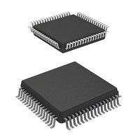
DF36034HJ Renesas Electronics America, DF36034HJ Datasheet - Page 28

DF36034HJ
Manufacturer Part Number
DF36034HJ
Description
MCU 3/5V 32K J-TEMP 64=QFP
Manufacturer
Renesas Electronics America
Series
H8® H8/300H Tinyr
Datasheet
1.DF36057GFZV.pdf
(594 pages)
Specifications of DF36034HJ
Core Processor
H8/300H
Core Size
16-Bit
Speed
20MHz
Connectivity
CAN, SCI, SSU
Peripherals
PWM, WDT
Number Of I /o
45
Program Memory Size
32KB (32K x 8)
Program Memory Type
FLASH
Ram Size
2K x 8
Voltage - Supply (vcc/vdd)
3 V ~ 5.5 V
Data Converters
A/D 8x10b
Oscillator Type
Internal
Operating Temperature
-40°C ~ 85°C
Package / Case
64-QFP
Lead Free Status / RoHS Status
Contains lead / RoHS non-compliant
Eeprom Size
-
Other names
HD64F36034HJ
HD64F36034HJ
HD64F36034HJ
- Current page: 28 of 594
- Download datasheet (4Mb)
Figure 15.15 Set Timing for Message Reception ....................................................................... 338
Figure 15.16 RXPR/RFPR Set/Clear Timing when Overrun/Overwrite Occurs........................ 339
Figure 15.17 Flowchart for Changing ID, MBCR, and LAFM of Receive Mailbox.................. 341
Figure 15.18 Flowchart for Transition between Active Mode and Standby Mode or Module
Standby Mode ....................................................................................................... 343
Figure 15.19 High-Speed CAN Bus Interface Using HA13721 ................................................. 346
Section 16 Synchronous Serial Communication Unit (SSU)
Figure 16.1 Block Diagram of SSU............................................................................................ 350
Figure 16.2 Relationship between Clock Polarity and Phase, and Data ..................................... 360
Figure 16.3 Relationship between Data Input/Output Pin and Shift Register ............................ 361
Figure 16.4 Initialization in Clocked Synchronous Communication Mode................................ 363
Figure 16.5 Example of Operation in Data Transmission .......................................................... 364
Figure 16.6 Sample Serial Transmission Flowchart ................................................................... 365
Figure 16.7 Example of Operation in Data Reception (MSS = 1) .............................................. 366
Figure 16.8 Sample Serial Reception Flowchart (MSS = 1)....................................................... 367
Figure 16.9 Sample Flowchart for Serial Transmit and Receive Operations.............................. 369
Figure 16.10 Initialization in Four-Line Bus Communication Mode ......................................... 371
Figure 16.11 Example of Operation in Data Transmission (MSS = 1)....................................... 373
Figure 16.12 Example of Operation in Data Reception (MSS = 1) ............................................ 375
Figure 16.13 Arbitration Check Timing ..................................................................................... 376
Figure 16.14 Procedures when Changing Output Level of Serial Data ...................................... 378
Section 17 Subsystem Timer (Subtimer)
Figure 17.1 Block Diagram of Subtimer .................................................................................... 380
Figure 17.2 Timing for On-Chip Oscillator................................................................................ 383
Figure 17.3 SBTPS Setting Flowchart........................................................................................ 385
Figure 17.4 Example of Subtimer Operation.............................................................................. 388
Figure 17.5 Count Operation Flowchart ..................................................................................... 389
Section 18 A/D Converter
Figure 18.1 Block Diagram of A/D Converter ........................................................................... 392
Figure 18.2 A/D Conversion Timing.......................................................................................... 398
Figure 18.3 External Trigger Input Timing ................................................................................ 399
Figure 18.4 A/D Conversion Accuracy Definitions (1).............................................................. 401
Figure 18.5 A/D Conversion Accuracy Definitions (2).............................................................. 401
Figure 18.6 Analog Input Circuit Example ................................................................................ 402
Section 19 Power-On Reset and Low-Voltage Detection Circuits (Optional)
Figure 19.1 Block Diagram of Power-On Reset Circuit and Low-Voltage Detection Circuit.... 404
Figure 19.2 Operational Timing of Power-On Reset Circuit...................................................... 409
Figure 19.3 Operational Timing of LVDR Circuit ..................................................................... 410
Rev. 4.00 Mar. 15, 2006 Page xxvi of xxxii
Related parts for DF36034HJ
Image
Part Number
Description
Manufacturer
Datasheet
Request
R

Part Number:
Description:
KIT STARTER FOR M16C/29
Manufacturer:
Renesas Electronics America
Datasheet:

Part Number:
Description:
KIT STARTER FOR R8C/2D
Manufacturer:
Renesas Electronics America
Datasheet:

Part Number:
Description:
R0K33062P STARTER KIT
Manufacturer:
Renesas Electronics America
Datasheet:

Part Number:
Description:
KIT STARTER FOR R8C/23 E8A
Manufacturer:
Renesas Electronics America
Datasheet:

Part Number:
Description:
KIT STARTER FOR R8C/25
Manufacturer:
Renesas Electronics America
Datasheet:

Part Number:
Description:
KIT STARTER H8S2456 SHARPE DSPLY
Manufacturer:
Renesas Electronics America
Datasheet:

Part Number:
Description:
KIT STARTER FOR R8C38C
Manufacturer:
Renesas Electronics America
Datasheet:

Part Number:
Description:
KIT STARTER FOR R8C35C
Manufacturer:
Renesas Electronics America
Datasheet:

Part Number:
Description:
KIT STARTER FOR R8CL3AC+LCD APPS
Manufacturer:
Renesas Electronics America
Datasheet:

Part Number:
Description:
KIT STARTER FOR RX610
Manufacturer:
Renesas Electronics America
Datasheet:

Part Number:
Description:
KIT STARTER FOR R32C/118
Manufacturer:
Renesas Electronics America
Datasheet:

Part Number:
Description:
KIT DEV RSK-R8C/26-29
Manufacturer:
Renesas Electronics America
Datasheet:

Part Number:
Description:
KIT STARTER FOR SH7124
Manufacturer:
Renesas Electronics America
Datasheet:

Part Number:
Description:
KIT STARTER FOR H8SX/1622
Manufacturer:
Renesas Electronics America
Datasheet:

Part Number:
Description:
KIT DEV FOR SH7203
Manufacturer:
Renesas Electronics America
Datasheet:


