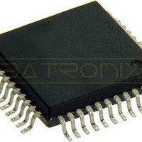
MC68HC705C9ACFBE Freescale Semiconductor, MC68HC705C9ACFBE Datasheet - Page 74

MC68HC705C9ACFBE
Manufacturer Part Number
MC68HC705C9ACFBE
Description
IC MCU 8BIT 44-QFP
Manufacturer
Freescale Semiconductor
Series
HC05r
Datasheet
1.MC705C9ACPE.pdf
(118 pages)
Specifications of MC68HC705C9ACFBE
Core Processor
HC05
Core Size
8-Bit
Speed
2.1MHz
Connectivity
SCI, SPI
Peripherals
POR, WDT
Number Of I /o
24
Program Memory Size
16KB (16K x 8)
Program Memory Type
OTP
Ram Size
352 x 8
Voltage - Supply (vcc/vdd)
3 V ~ 5.5 V
Oscillator Type
Internal
Operating Temperature
-40°C ~ 85°C
Package / Case
44-QFP
Processor Series
HC705C
Core
HC05
Data Bus Width
8 bit
Data Ram Size
352 B
Interface Type
SCI, SPI
Maximum Clock Frequency
2.1 MHz
Number Of Programmable I/os
31
Number Of Timers
1
Maximum Operating Temperature
+ 85 C
Mounting Style
SMD/SMT
Minimum Operating Temperature
- 40 C
On-chip Adc
8 bit
Package
44PQFP
Family Name
HC05
Maximum Speed
2.1 MHz
Operating Supply Voltage
3.3|5 V
Lead Free Status / RoHS Status
Lead free / RoHS Compliant
Eeprom Size
-
Data Converters
-
Lead Free Status / Rohs Status
Details
Available stocks
Company
Part Number
Manufacturer
Quantity
Price
Company:
Part Number:
MC68HC705C9ACFBE
Manufacturer:
FREESCALE
Quantity:
1 827
Company:
Part Number:
MC68HC705C9ACFBE
Manufacturer:
Freescale Semiconductor
Quantity:
10 000
Serial Peripheral Interface (SPI)
The SPI is double buffered on read, but not on write. If a write is performed during data transfer, the
transfer occurs uninterrupted, and the write will be unsuccessful. This condition will cause the write
collision (WCOL) status bit in the SPSR to be set. After a data byte is shifted, the SPIF flag of the SPSR
is set.
In the master mode, the SCK pin is an output. It idles high or low, depending on the CPOL bit in the SPCR,
until data is written to the shift register, at which point eight clocks are generated to shift the eight bits of
data and then SCK goes idle again.
In a slave mode, the slave select start logic receives a logic low at the SS pin and a clock at the SCK pin.
Thus, the slave is synchronized with the master. Data from the master is received serially at the MOSI
line and loads the 8-bit shift register. After the 8-bit shift register is loaded, its data is parallel transferred
to the read buffer. During a write cycle, data is written into the shift register, then the slave waits for a clock
train from the master to shift the data out on the slave’s MISO line.
Figure 10-3
10.5 SPI Registers
Three registers in the SPI provide control, status, and data storage functions. These registers are called
the serial peripheral control register (SPCR), serial peripheral status register (SPSR), and serial
peripheral data I/O register (SPDR) and are described in the following paragraphs.
10.5.1 Serial Peripheral Control Register
The SPI control register (SPCR), shown in
74
•
•
•
•
•
•
Enables SPI interrupts
Enables the SPI system
Selects between standard CMOS or open drain outputs for port D (C9A mode only)
Selects between master mode and slave mode
Controls the clock/data relationship between master and slave
Determines the idle level of the clock pin
illustrates the MOSI, MISO, SCK, and SS master-slave interconnections.
Figure 10-3. Serial Peripheral Interface Master-Slave Interconnection
SPI SHIFT REGISTER
7 6 5 4 3 2 1 0
MASTER MCU
SPDR ($000C)
MC68HC05C9A Advance Information Data Sheet, Rev. 4.1
I/O PORT
Figure
PD3/MOSI
PD2/MISO
PD4/SCK
10-4, controls these functions:
PD5/SS
SLAVE MCU
SPI SHIFT REGISTER
7 6 5 4 3 2 1 0
SPDR ($000C)
Freescale Semiconductor


