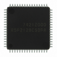
R5F212BCSDFA#U0 Renesas Electronics America, R5F212BCSDFA#U0 Datasheet - Page 42

R5F212BCSDFA#U0
Manufacturer Part Number
R5F212BCSDFA#U0
Description
IC R8C/2B MCU FLASH 64LQFP
Manufacturer
Renesas Electronics America
Series
R8C/2x/2Br
Datasheet
1.R5F212B7SNFPU0.pdf
(66 pages)
Specifications of R5F212BCSDFA#U0
Core Size
16/32-Bit
Program Memory Size
128KB (128K x 8)
Peripherals
POR, PWM, Voltage Detect, WDT
Core Processor
R8C
Speed
20MHz
Connectivity
I²C, LIN, SIO, SSU, UART/USART
Number Of I /o
55
Program Memory Type
FLASH
Ram Size
7.5K x 8
Voltage - Supply (vcc/vdd)
2.2 V ~ 5.5 V
Data Converters
A/D 12x10b; D/A 2x8b
Oscillator Type
Internal
Operating Temperature
-40°C ~ 85°C
Package / Case
64-LQFP
No. Of I/o's
55
Ram Memory Size
7.5KB
Cpu Speed
20MHz
No. Of Timers
6
Digital Ic Case Style
LQFP
Embedded Interface Type
I2C, UART
Rohs Compliant
Yes
Lead Free Status / RoHS Status
Lead free / RoHS Compliant
For Use With
R0K5212D8S001BE - KIT STARTER FOR R8C/2DR0K5212D8S000BE - KIT DEV FOR R8C/2D
Eeprom Size
-
Lead Free Status / RoHS Status
Lead free / RoHS Compliant, Lead free / RoHS Compliant
Available stocks
Company
Part Number
Manufacturer
Quantity
Price
R8C/2A Group, R8C/2B Group
Rev.2.10
REJ03B0182-0210
Figure 5.3
Table 5.10
NOTES:
V
V
t
rth
reset signal
por1
por2
Power V
Symbol
NOTES:
1. The measurement condition is T
2. This condition (external power VCC rise gradient) does not apply if V
3. To use the power-on reset function, enable voltage monitor 0 reset by setting the LVD0ON bit in the OFS register to 0, the
4. t
(“L” valid)
External
Internal
1. When using the voltage monitor 0 digital filter, ensure that the voltage is within the MCU operation voltage
2. The sampling clock can be selected. Refer to 6. Voltage Detection Circuit of Hardware Manual for details.
3. V
V
VW0C0 and VW0C6 bits in the VW0C register to 1 respectively, and the VCA25 bit in the VCA2 register to 1.
reset. When turning on the power for the first time, maintain t
3,000 s or more if −40°C ≤ T
w(por1)
V
det0
por1
range (2.2 V or above) during the sampling time.
Circuit of Hardware Manual for details.
Nov 26, 2007
CC
det0
(3)
indicates the duration the external power V
Power-on reset valid voltage
Power-on reset or voltage monitor 0 reset valid
voltage
External power V
indicates the voltage detection level of the voltage detection 0 circuit. Refer to 6. Voltage Detection
Power-on Reset Circuit, Voltage Monitor 0 Reset Electrical Characteristics
Power-on Reset Circuit Electrical Characteristics
t
w(por1)
Page 40 of 60
CC
Parameter
rise gradient
t
opr
rth
< −20°C.
opr
= -20 to 85°C (N version) / -40 to 85°C (D version), unless otherwise specified.
(4)
(2)
f
OCO-S
1
CC
Sampling time
× 32
must be held below the effective voltage (V
w(por1)
Condition
for 30 s or more if −20°C ≤ T
(1, 2)
CC
≥ 1.0 V.
2.2V
t
rth
Min.
20
−
0
5. Electrical Characteristics
Standard
opr
f
Typ.
OCO-S
≤ 85°C, maintain t
por1
V
−
−
−
1
por2
) to enable a power on
× 32
Max.
V
0.1
det0
−
V
det0
(3)
(3)
mV/msec
w(por1)
Unit
V
V
for


