R5F2L3AAANFP#U1 Renesas Electronics America, R5F2L3AAANFP#U1 Datasheet - Page 666
R5F2L3AAANFP#U1
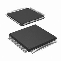
Manufacturer Part Number
R5F2L3AAANFP#U1
Description
MCU FLASH 96+4KB 100LQFP
Manufacturer
Renesas Electronics America
Series
R8C/Lx/3AAr
Datasheet
1.R5F2L387ANFPU1.pdf
(864 pages)
Specifications of R5F2L3AAANFP#U1
Core Processor
R8C
Core Size
16/32-Bit
Speed
20MHz
Connectivity
I²C, LIN, SIO, SSU, UART/USART
Peripherals
LCD, POR, PWM, Voltage Detect, WDT
Number Of I /o
88
Program Memory Size
96KB (96K x 8)
Program Memory Type
FLASH
Ram Size
10K x 8
Voltage - Supply (vcc/vdd)
1.8 V ~ 5.5 V
Data Converters
A/D 20x10b; D/A 2x8b
Oscillator Type
Internal
Operating Temperature
-20°C ~ 85°C
Package / Case
100-LQFP
Lead Free Status / RoHS Status
Lead free / RoHS Compliant
Eeprom Size
-
Available stocks
Company
Part Number
Manufacturer
Quantity
Price


R8C/L35A Group, R8C/L36A Group, R8C/L38A Group, R8C/L3AA Group,
R8C/L35B Group, R8C/L36B Group, R8C/L38B Group, R8C/L3AB Group
REJ09B0441-0100 Rev.1.00
Page 629 of 802
29. A/D Converter
29.1
The description offered in this chapter is based on the R8C/L3AA Group and the R8C/L3AB Group.
For other groups, refer to 1.1.2 Differences between Groups.
Table 29.1
Notes:
A/D conversion method
Analog input voltage
Operating clock AD
Resolution
Absolute accuracy
Operating modes
Analog input pins
A/D conversion
start conditions
Conversion rate per pin
( AD = fAD)
The A/D converter consists of one 10-bit successive approximation A/D converter circuit with a capacitive
coupling amplifier. The analog input shares pins P0_0 to P0_7, P1_0 to P1_3, and P13_0 to P13_7.
Table 29.1 lists the A/D Converter Performance. Figure 29.1 shows the A/D Converter Block Diagram.
Note
1. When the analog input voltage is over the reference voltage, the A/D conversion result will be 3FFh in 10-bit
2. When 4.0 V
3. The conversion rate per pin is minimum 43 AD cycles for 8-bit and 10-bit resolution.
mode and FFh in 8-bit mode.
When 3.2 V
When 2.7 V
When 2.2 V
The frequency of AD must be 2 MHz or above.
Introduction
Item
A/D Converter Performance
AVCC
AVCC < 5.5 V, the frequency of AD must be 16 MHz or below.
AVCC < 5.5 V, the frequency of AD must be 10 MHz or below.
AVCC < 5.5 V, the frequency of AD must be 5 MHz or below.
(1)
(2)
(3)
5.5 V, the frequency of AD must be 20 MHz or below.
Oct 30, 2009
Successive approximation (with capacitive coupling amplifier)
0 V to AVCC
fAD, fAD divided by 2, fAD divided by 4, fAD divided by 8 (fAD = f1)
8 bits or 10 bits selectable
AVCC = Vref = 5 V, AD = 20 MHz
AVCC = Vref = 3.3 V, AD = 16 MHz
AVCC = Vref = 3.0 V, AD = 10 MHz
AVCC = Vref = 2.2 V, AD = 5 MHz
One-shot mode, repeat mode 0, repeat mode 1, single sweep mode, and repeat
sweep mode
20 pins (AN0 to AN19)
• Software trigger
• Timer RD
• Timer RC
• External trigger
Minimum 43 AD cycles
(Refer to 29.3.3 A/D Conversion Start Conditions .)
• 8-bit resolution
• 10-bit resolution
• 8-bit resolution
• 10-bit resolution
• 8-bit resolution
• 10-bit resolution
• 8-bit resolution
• 10-bit resolution
±2 LSB
±3 LSB
±2 LSB
±5 LSB
±2 LSB
±5 LSB
±2 LSB
±5 LSB
Performance
29. A/D Converter
Related parts for R5F2L3AAANFP#U1
Image
Part Number
Description
Manufacturer
Datasheet
Request
R

Part Number:
Description:
KIT STARTER FOR M16C/29
Manufacturer:
Renesas Electronics America
Datasheet:

Part Number:
Description:
KIT STARTER FOR R8C/2D
Manufacturer:
Renesas Electronics America
Datasheet:

Part Number:
Description:
R0K33062P STARTER KIT
Manufacturer:
Renesas Electronics America
Datasheet:

Part Number:
Description:
KIT STARTER FOR R8C/23 E8A
Manufacturer:
Renesas Electronics America
Datasheet:

Part Number:
Description:
KIT STARTER FOR R8C/25
Manufacturer:
Renesas Electronics America
Datasheet:

Part Number:
Description:
KIT STARTER H8S2456 SHARPE DSPLY
Manufacturer:
Renesas Electronics America
Datasheet:

Part Number:
Description:
KIT STARTER FOR R8C38C
Manufacturer:
Renesas Electronics America
Datasheet:

Part Number:
Description:
KIT STARTER FOR R8C35C
Manufacturer:
Renesas Electronics America
Datasheet:

Part Number:
Description:
KIT STARTER FOR R8CL3AC+LCD APPS
Manufacturer:
Renesas Electronics America
Datasheet:
Part Number:
Description:
KIT STARTER FOR RX610
Manufacturer:
Renesas Electronics America
Datasheet:

Part Number:
Description:
KIT STARTER FOR R32C/118
Manufacturer:
Renesas Electronics America
Datasheet:

Part Number:
Description:
KIT DEV RSK-R8C/26-29
Manufacturer:
Renesas Electronics America
Datasheet:

Part Number:
Description:
KIT STARTER FOR SH7124
Manufacturer:
Renesas Electronics America
Datasheet:

Part Number:
Description:
KIT STARTER FOR H8SX/1622
Manufacturer:
Renesas Electronics America
Datasheet:

Part Number:
Description:
KIT DEV FOR SH7203
Manufacturer:
Renesas Electronics America
Datasheet: