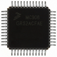
MC908GR32ACFAE Freescale Semiconductor, MC908GR32ACFAE Datasheet - Page 252

MC908GR32ACFAE
Manufacturer Part Number
MC908GR32ACFAE
Description
IC MCU 32K FLASH 8MHZ 48-LQFP
Manufacturer
Freescale Semiconductor
Series
HC08r
Datasheet
1.MC908GR32ACFJE.pdf
(314 pages)
Specifications of MC908GR32ACFAE
Core Processor
HC08
Core Size
8-Bit
Speed
8MHz
Connectivity
SCI, SPI
Peripherals
LVD, POR, PWM
Number Of I /o
37
Program Memory Size
32KB (32K x 8)
Program Memory Type
FLASH
Ram Size
1.5K x 8
Voltage - Supply (vcc/vdd)
3 V ~ 5.5 V
Data Converters
A/D 24x10b
Oscillator Type
Internal
Operating Temperature
-40°C ~ 85°C
Package / Case
48-LQFP
Controller Family/series
HC08
No. Of I/o's
37
Ram Memory Size
1.5KB
Cpu Speed
8MHz
No. Of Timers
2
Embedded Interface Type
SCI, SPI
Rohs Compliant
Yes
Processor Series
HC08GR
Core
HC08
Data Bus Width
8 bit
Data Ram Size
1.5 KB
Interface Type
ESCI, SPI
Maximum Clock Frequency
8 MHz
Number Of Programmable I/os
53
Number Of Timers
8
Maximum Operating Temperature
+ 85 C
Mounting Style
SMD/SMT
Development Tools By Supplier
FSICEBASE, DEMO908GZ60E, M68CBL05CE, M68EML08GPGTE
Minimum Operating Temperature
- 40 C
On-chip Adc
10 bit, 24 Channel
Lead Free Status / RoHS Status
Lead free / RoHS Compliant
Eeprom Size
-
Lead Free Status / Rohs Status
Details
Available stocks
Company
Part Number
Manufacturer
Quantity
Price
Company:
Part Number:
MC908GR32ACFAE
Manufacturer:
Freescale Semiconductor
Quantity:
10 000
Company:
Part Number:
MC908GR32ACFAER
Manufacturer:
Freescale Semiconductor
Quantity:
10 000
- Current page: 252 of 314
- Download datasheet (5Mb)
Timer Interface Module (TIM2)
18.7 I/O Signals
Port D shares two of its pins with the TIM2. Port F shares four of its pins with the TIM2. PTD6/T2CH0 is
an external clock input to the TIM2 prescaler. The six TIM2 channel I/O pins are PTD6/T2CH0,
PTD7/T2CH1, PTF4/T2CH2, PTF5/T2CH3, PTF6/T2CH4, and PTF7/T2CH5.
18.7.1 TIM2 Clock Pin (T2CH0)
T2CH0 is an external clock input that can be the clock source for the TIM2 counter instead of the
prescaled internal bus clock. Select the T2CH0 input by writing 1s to the three prescaler select bits,
PS[2:0]. (See
20.14 Timer Interface Module
frequency ÷ 2.
When the PTD6/T2CH0 pin is the TIM2 clock input, it is an input regardless of the state of the DDRD6 bit
in data direction register D.
18.7.2 TIM2 Channel I/O Pins (T2CH5:T2CH2 and T2CH1:T2CH0)
Each channel I/O pin is programmable independently as an input capture pin or an output compare pin.
T2CH0, T2CH2, and T2CH4 can be configured as buffered output compare or buffered PWM pins.
18.8 I/O Registers
These I/O registers control and monitor TIM2 operation:
18.8.1 TIM2 Status and Control Register
The TIM2 status and control register:
252
•
•
•
•
•
•
•
•
•
•
TIM2 status and control register (T2SC)
TIM2 counter registers (T2CNTH:T2CNTL)
TIM2 counter modulo registers (T2MODH:T2MODL)
TIM2 channel status and control registers (T2SC0, T2SC1, T2SC2, T2SC3, T2SC4, and T2SC5)
TIM2 channel registers (T2CH0H:T2CH0L, T2CH1H:T2CH1L, T2CH2H:T2CH2L,
T2CH3H:T2CH3L, T2CH4H:T2CH4L, and T2CH5H:T2CH5L)
Enables TIM2 overflow interrupts
Flags TIM2 overflows
Stops the TIM2 counter
Resets the TIM2 counter
Prescales the TIM2 counter clock
18.8.1 TIM2 Status and Control
Address:
Reset:
Read:
Write:
MC68HC908GR60A • MC68HC908GR48A • MC68HC908GR32A Data Sheet, Rev. 5
$002B
Figure 18-5. TIM2 Status and Control Register (T2SC)
Bit 7
TOF
0
0
Characteristics. The maximum TCLK frequency is the least: 4 MHz or bus
= Unimplemented
TOIE
6
0
TSTOP
5
1
Register.) The minimum TCLK pulse width is specified in
TRST
4
0
0
3
0
0
PS2
2
0
PS1
1
0
Freescale Semiconductor
Bit 0
PS0
0
Related parts for MC908GR32ACFAE
Image
Part Number
Description
Manufacturer
Datasheet
Request
R
Part Number:
Description:
Manufacturer:
Freescale Semiconductor, Inc
Datasheet:
Part Number:
Description:
Manufacturer:
Freescale Semiconductor, Inc
Datasheet:
Part Number:
Description:
Manufacturer:
Freescale Semiconductor, Inc
Datasheet:
Part Number:
Description:
Manufacturer:
Freescale Semiconductor, Inc
Datasheet:
Part Number:
Description:
Manufacturer:
Freescale Semiconductor, Inc
Datasheet:
Part Number:
Description:
Manufacturer:
Freescale Semiconductor, Inc
Datasheet:
Part Number:
Description:
Manufacturer:
Freescale Semiconductor, Inc
Datasheet:
Part Number:
Description:
Manufacturer:
Freescale Semiconductor, Inc
Datasheet:
Part Number:
Description:
Manufacturer:
Freescale Semiconductor, Inc
Datasheet:
Part Number:
Description:
Manufacturer:
Freescale Semiconductor, Inc
Datasheet:
Part Number:
Description:
Manufacturer:
Freescale Semiconductor, Inc
Datasheet:
Part Number:
Description:
Manufacturer:
Freescale Semiconductor, Inc
Datasheet:
Part Number:
Description:
Manufacturer:
Freescale Semiconductor, Inc
Datasheet:
Part Number:
Description:
Manufacturer:
Freescale Semiconductor, Inc
Datasheet:
Part Number:
Description:
Manufacturer:
Freescale Semiconductor, Inc
Datasheet:


