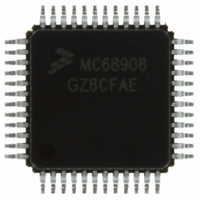
MC68908GZ8CFAE Freescale Semiconductor, MC68908GZ8CFAE Datasheet - Page 27

MC68908GZ8CFAE
Manufacturer Part Number
MC68908GZ8CFAE
Description
IC MCU 8K FLASH 8MHZ CAN 48-LQFP
Manufacturer
Freescale Semiconductor
Series
HC08r
Datasheet
1.MC68908GZ8CFJER.pdf
(314 pages)
Specifications of MC68908GZ8CFAE
Core Processor
HC08
Core Size
8-Bit
Speed
8MHz
Connectivity
CAN, LIN, SCI, SPI
Peripherals
LVD, POR, PWM
Number Of I /o
37
Program Memory Size
8KB (8K x 8)
Program Memory Type
FLASH
Ram Size
1K x 8
Voltage - Supply (vcc/vdd)
3 V ~ 5.5 V
Data Converters
A/D 8x10b
Oscillator Type
Internal
Operating Temperature
-40°C ~ 85°C
Package / Case
48-LQFP
Processor Series
M689xx
Core
HC08
Data Bus Width
8 bit
Data Ram Size
1024 B
Interface Type
ESCI, SPI, UART
Maximum Clock Frequency
8 MHz
Number Of Programmable I/os
37
Number Of Timers
2
Operating Supply Voltage
0 V to 5.5 V
Maximum Operating Temperature
+ 85 C
Mounting Style
SMD/SMT
Development Tools By Supplier
FSICEBASE, M68CBL05AE, DEMO908GZ60E, M68EML08GZE
Minimum Operating Temperature
- 40 C
On-chip Adc
10 bit, 8 Channel
Package
48LQFP
Family Name
HC08
Maximum Speed
8 MHz
Lead Free Status / RoHS Status
Lead free / RoHS Compliant
Eeprom Size
-
Lead Free Status / Rohs Status
Details
Available stocks
Company
Part Number
Manufacturer
Quantity
Price
Company:
Part Number:
MC68908GZ8CFAE
Manufacturer:
Renesas
Quantity:
301
Company:
Part Number:
MC68908GZ8CFAE
Manufacturer:
Freescale Semiconductor
Quantity:
10 000
Part Number:
MC68908GZ8CFAE
Manufacturer:
FREESCALE
Quantity:
20 000
- Current page: 27 of 314
- Download datasheet (5Mb)
Chapter 2
Memory
2.1 Introduction
The CPU08 can address 64 Kbytes of memory space. The memory map, shown in
2.2 Unimplemented Memory Locations
Accessing an unimplemented location can cause an illegal address reset. In the memory map
(Figure
2.3 Reserved Memory Locations
Accessing a reserved location can have unpredictable effects on microcontroller (MCU) operation. In the
Figure 2-1
or with the letter R.
2.4 Input/Output (I/O) Section
Most of the control, status, and data registers are in the zero page area of $0000–$003F. Additional I/O
registers have these addresses:
Data registers are shown in
Freescale Semiconductor
•
•
•
•
•
•
•
•
•
•
•
•
•
•
•
•
•
•
•
15,872 bytes of user FLASH memory
1024 bytes of random-access memory (RAM)
406 bytes of FLASH programming routines read-only memory (ROM)
44 bytes of user-defined vectors
350 bytes of monitor ROM
$FE00; break status register, SBSR
$FE01; SIM reset status register, SRSR
$FE02; break auxiliary register, BRKAR
$FE03; break flag control register, BFCR
$FE04; interrupt status register 1, INT1
$FE05; interrupt status register 2, INT2
$FE06; interrupt status register 3, INT3
$FE07; reserved
$FE08; FLASH control register, FLCR
$FE09; break address register high, BRKH
$FE0A; break address register low, BRKL
$FE0B; break status and control register, BRKSCR
$FE0C; LVI status register, LVISR
$FF7E; FLASH block protect register, FLBPR
2-1) and in register figures in this document, unimplemented locations are shaded.
and in register figures in this document, reserved locations are marked with the word Reserved
MC68HC908GZ16 • MC68HC908GZ8 Data Sheet, Rev. 4
Figure
2-2.
Table 2-1
is a list of vector locations.
Figure
2-1, includes:
27
Related parts for MC68908GZ8CFAE
Image
Part Number
Description
Manufacturer
Datasheet
Request
R
Part Number:
Description:
Manufacturer:
Freescale Semiconductor, Inc
Datasheet:
Part Number:
Description:
Manufacturer:
Freescale Semiconductor, Inc
Datasheet:
Part Number:
Description:
Manufacturer:
Freescale Semiconductor, Inc
Datasheet:
Part Number:
Description:
Manufacturer:
Freescale Semiconductor, Inc
Datasheet:
Part Number:
Description:
Manufacturer:
Freescale Semiconductor, Inc
Datasheet:
Part Number:
Description:
Manufacturer:
Freescale Semiconductor, Inc
Datasheet:
Part Number:
Description:
Manufacturer:
Freescale Semiconductor, Inc
Datasheet:
Part Number:
Description:
Manufacturer:
Freescale Semiconductor, Inc
Datasheet:
Part Number:
Description:
Manufacturer:
Freescale Semiconductor, Inc
Datasheet:
Part Number:
Description:
Manufacturer:
Freescale Semiconductor, Inc
Datasheet:
Part Number:
Description:
Manufacturer:
Freescale Semiconductor, Inc
Datasheet:
Part Number:
Description:
Manufacturer:
Freescale Semiconductor, Inc
Datasheet:
Part Number:
Description:
Manufacturer:
Freescale Semiconductor, Inc
Datasheet:
Part Number:
Description:
Manufacturer:
Freescale Semiconductor, Inc
Datasheet:
Part Number:
Description:
Manufacturer:
Freescale Semiconductor, Inc
Datasheet:


