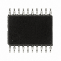
R5F211B1SP#U0 Renesas Electronics America, R5F211B1SP#U0 Datasheet - Page 21

R5F211B1SP#U0
Manufacturer Part Number
R5F211B1SP#U0
Description
IC R8C MCU FLASH 4K 20SSOP
Manufacturer
Renesas Electronics America
Series
M16C™ M16C/R8C/Tiny/1Br
Datasheets
1.R5F211A2SPU0.pdf
(51 pages)
2.R5F211A2SPU0.pdf
(300 pages)
3.R5F211A2SPU0.pdf
(341 pages)
Specifications of R5F211B1SP#U0
Core Processor
R8C
Core Size
16-Bit
Speed
20MHz
Connectivity
I²C, SIO, SSU, UART/USART
Peripherals
LED, POR, Voltage Detect, WDT
Number Of I /o
13
Program Memory Size
4KB (4K x 8)
Program Memory Type
FLASH
Ram Size
384 x 8
Voltage - Supply (vcc/vdd)
2.7 V ~ 5.5 V
Data Converters
A/D 4x10b
Oscillator Type
Internal
Operating Temperature
-20°C ~ 85°C
Package / Case
20-SSOP
For Use With
R0K5211B4S001BE - KIT STARTER FOR R8C/18191A1BR0K5211B4S000BE - KIT DEV EVALUATION R8C/1BR0E521174CPE10 - EMULATOR COMPACT R8C/18/19/1
Lead Free Status / RoHS Status
Lead free / RoHS Compliant
Eeprom Size
-
Available stocks
Company
Part Number
Manufacturer
Quantity
Price
R8C/1A Group, R8C/1B Group
Rev.1.40
REJ03B0144-0140
3.2
Figure 3.2
Figure 3.2 is a Memory Map of R8C/1B Group. The R8C/1B Group has 1 Mbyte of address space from
addresses 00000h to FFFFFh.
The internal ROM (program ROM) is allocated lower addresses, beginning with address 0FFFFh. For
example, a 16-Kbyte internal ROM area is allocated addresses 0C000h to 0FFFFh.
The fixed interrupt vector table is allocated addresses 0FFDCh to 0FFFFh. They store the starting
address of each interrupt routine.
The internal ROM (data flash) is allocated addresses 02400h to 02BFFh.
The internal RAM is allocated higher addresses beginning with address 00400h. For example, a 1-
Kbyte internal RAM area is allocated addresses 00400h to 007FFh. The internal RAM is used not only
for storing data but also for calling subroutines and as stacks when interrupt requests are
acknowledged.
Special function registers (SFRs) are allocated addresses 00000h to 002FFh. The peripheral function
control registers are allocated here. All addresses within the SFR, which have nothing allocated are
reserved for future use and cannot be accessed by users.
R5F211B4SP, R5F211B4DSP, R5F211B4DD, R5F211B4NP,
R5F211B4XXXSP, R5F211B4DXXXSP, R5F211B4XXXDD,
R5F211B4XXXNP
R5F211B3SP, R5F211B3DSP, R5F211B3DD, R5F211B3NP,
R5F211B3XXXSP, R5F211B3DXXXSP, R5F211B3XXXDD,
R5F211B3XXXNP
R5F211B2SP, R5F211B2DSP, R5F211B2DD, R5F211B2NP,
R5F211B2XXXSP, R5F211B2DXXXSP, R5F211B2XXXDD,
R5F211B2XXXNP
R5F211B1SP, R5F211B1DSP, R5F211B1DD,
R5F211B1XXXSP, R5F211B1DXXXSP, R5F211B1XXXDD
R8C/1B Group
Dec 08, 2006
0XXXXh
0YYYYh
FFFFFh
02BFFh
0FFFFh
002FFh
00000h
00400h
02400h
Memory Map of R8C/1B Group
(See 4. Special Function
NOTES:
1. Data flash block A (1 Kbyte) and B (1 Kbyte) are shown.
2. The blank regions are reserved. Do not access locations in these regions.
Registers (SFRs))
(program ROM)
Expanded area
(data Flash)
Internal ROM
Internal ROM
Internal RAM
Part Number
SFR
Page 19 of 45
(1)
0FFDCh
0FFFFh
16 Kbytes
12 Kbytes
8 Kbytes
4 Kbytes
Size
Watchdog timer • oscillation stop detection • voltage monitor 2
Internal ROM
0YYYYh
Address
0C000h
0D000h
0E000h
0F000h
Undefined instruction
BRK instruction
Address match
Address break
Single step
(Reserved)
Overflow
Reset
768 bytes
384 bytes
512 bytes
1 Kbyte
Size
Internal RAM
0XXXXh
Address
007FFh
006FFh
005FFh
0057Fh
3. Memory


